SLUSCP1A August 2016 – August 2016
PRODUCTION DATA.
- 1 Features
- 2 Applications
- 3 Description
- 4 Revision History
- 5 Pin Configuration and Functions
- 6 Specifications
- 7 Detailed Description
- 8 Application and Implementation
- 9 Power Supply Recommendations
- 10Layout
- 11Device and Documentation Support
- 12Mechanical, Packaging, and Orderable Information
Package Options
Mechanical Data (Package|Pins)
- RHB|32
Thermal pad, mechanical data (Package|Pins)
- RHB|32
Orderable Information
1 Features
- 5-V Transmitter AFE Compatible With Wireless Power Consortium (WPC) v1.2 A11 Low-Power Transmitter Specification
- Designed to be Used With bq500511A WPC Controller
- Note: The bq50002A is Incompatible With the bq500511 Device if Foreign Object Detection is Required
- Suitable for WPC and Proprietary 5-V Wireless Power Transmitters
- Supports 5 W on the Receiver Output
- Integrates All the Analog Functions Required in a Wireless Power Transmitter
- MOSFET Drivers and Synchronous N-Channel Power FETs
- Accurate Current Sense
- Variable Frequency Oscillator
- High-Efficiency Voltage Regulator
- High-Sensitivity Demodulator to Decode Signals From Receiver
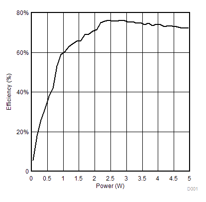
- 2-Chip Solution Enables High-Efficiency Transmitter Designs of >75% Efficiency
- Ultra-Low-Standby Power, Even During Digital Ping (<30 mW)
- Dynamic Power Limiting (DPL)™ Enables Operation From Input Sources With Limited Power
- System LED Indication of Charging State and Fault Status
- Accurate Foreign Object Detection Method (FOD)
2 Applications
- WPC Compliant Wireless Transmitters for Smart Phones and Wearable Applications
- Proprietary Wireless Chargers and Transmitters
- Medical and Wearable Applications
3 Description
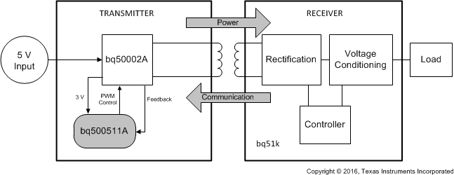
The bq50002A device is a highly integrated wireless power transmitter analog front end (AFE) that contains all of the analog components required to implement a Wireless Power Consortium (WPC) compliant 5-V transmitter. The bq50002A device integrates a full-bridge power driver with MOSFETs, variable-frequency oscillator, two-channel communication demodulator, linear regulator, and protection circuits. The bq50002A device must be used together with the digital controller bq500511A to realize a compact two chip wireless power transmitter solution. The bq500511A safely engages the RX device, receives packet communication from the powered device, and manages the power transfer according to WPC v1.2 specification.
The system supports foreign object detection (FOD) by continuously monitoring the amount of power transferred and comparing that to the amount of received power, as reported by the receiver. This protects against power loss to metal objects misplaced in the wireless power transfer field. To do this, the bq50002A measures the input DC current accurately by using a current sense amplifier. Should any abnormal condition develop during power transfer, the bq500511A handles it and provides indication outputs. Comprehensive status and fault monitoring features enable a low cost yet robust WPC-certified wireless power system design.
The bq50002A is available in a thermally enhanced 5.00 mm × 5.00 mm, 32-pin QFN package.
Device Information (1)
| PART NUMBER | PACKAGE | BODY SIZE (NOM) |
|---|---|---|
| bq50002A | QFN (32) | 5.00 mm × 5.00 mm |
- For all available packages, see the orderable addendum at the end of the data sheet.
Simplified Schematic

Efficiency vs Power
