SBOS765 January 2016
PRODUCTION DATA.
- 1 Features
- 2 Applications
- 3 Description
- 4 Revision History
- 5 Pin Configuration and Functions
- 6 Specifications
- 7 Detailed Description
- 8 Application and Implementation
- 9 Power Supply Recommendations
- 10Layout
- 11Device and Documentation Support
- 12Mechanical, Packaging, and Orderable Information
Package Options
Mechanical Data (Package|Pins)
- DCK|6
Thermal pad, mechanical data (Package|Pins)
Orderable Information
1 Features
- Wide Common-Mode Range: 0 V to 20 V
- Offset Voltage: ±150 μV (Maximum)
- Enables Shunt Drops of 10-mV Full-Scale
- Accuracy: ±2% Gain Error (Maximum Overtemperature)
- Fixed Gain: 50 V/V
- Low Quiescent Current: 100 μA (Maximum)
- Small Package: SC70
2 Applications
- WPC (Qi) 1.2-Compliant Wireless Power Transmitters for 15-W or 5-W Systems
- Proprietary Wireless Chargers and Transmitters
- Wirelessly-Powered Industrial and Medical Systems
- For more information, see www.ti.com/wirelesspower
3 Description
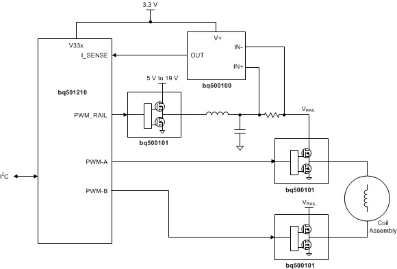
The bq500100 is a voltage output, current-shunt monitor for wireless charging to facilitate foreign object detection (FOD). This device can sense drops across shunts at common-mode voltages from 0 V to 20 V, independent of the supply voltage. The device features a fixed voltage gain of 50 V/V with a maximum gain error of 2% and a offset voltage of 150 μV (maximum).
This device operates from a single 2.7-V to 6-V power supply, drawing a maximum of 100 μA of supply current. The device is specified from –40°C to +105°C and is offered in the SC70 package.
Device Information(1)
| PART NUMBER | PACKAGE | BODY SIZE (NOM) |
|---|---|---|
| bq500100 | SC70 (6) | 2.00 mm × 1.25 mm |
- For all available packages, see the orderable addendum at the end of the data sheet.
Typical Wireless Charging Application
