SLUSBD6D July 2013 – July 2016
PRODUCTION DATA.
- 1 Features
- 2 Applications
- 3 Description
- 4 Revision History
- 5 Pin Configuration and Functions
- 6 Specifications
-
7 Detailed Description
- 7.1 Overview
- 7.2 Functional Block Diagram
- 7.3 Feature Description
- 7.4 Device Functional Modes
- 7.5 Programming
- 8 Application and Implementation
- 9 Power Supply Recommendations
- 10Layout
- 11Device and Documentation Support
- 12Mechanical, Packaging, and Orderable Information
Package Options
Mechanical Data (Package|Pins)
- RGZ|48
Thermal pad, mechanical data (Package|Pins)
- RGZ|48
Orderable Information
1 Features
- Proven, Qi-Certified Value Solution for Transmit-Side Application
- Lowest Device Count for Full WPC1.1 5-V Solution
- 5-V Operation Conforms to Wireless Power Consortium (WPC1.1) Type A5 or A11 Transmitter Specification
- Fully WPC Compliant, Including Improved Foreign Object Detection (FOD) Method
- Permits X7R Type Resonant Capacitors for Reduced Cost
- Dynamic Power Limiting™ for USB and Limited Source Operation
- Digital Demodulation Reduces Components
- LED Indication of Charging State and Fault Status
- Low Standby and High Efficiency
2 Applications
- Wireless Power Consortium (WPC1.1) Compliant Wireless Chargers for:
- Qi-Certified Smart Phones and Other Handhelds
- Car and Other Vehicle Accessories
- See www.ti.com/wirelesspower for more information on TI's Wireless Charging Solutions
3 Description
The bq500212A is a Qi-certified value solution that integrates all functions required to control wireless power delivery to a single WPC1.1 compliant receiver. It is WPC1.1 compliant and designed for 5-V systems as a wireless power consortium type A5 or A11 transmitter. The bq500212A pings the surrounding environment for WPC compliant devices to be powered, safely engages the device, receives packet communication from the powered device and manages the power transfer according to WPC1.1 specification. To maximize flexibility in wireless power control applications, Dynamic Power Limiting (DPL) is featured on the bq500212A. Dynamic Power Limiting enhances user experience by seamlessly optimizing the usage of power available from limited input supplies.
The bq500212A supports both foreign object detection (FOD) and enhanced parasitic metal object detection (PMOD) for legacy product by continuously monitoring the efficiency of the established power transfer, protecting from power loss due to metal objects misplaced in the wireless power transfer field. The bq500212A handles any abnormal condition development during power transfer and provides indicator outputs. Comprehensive status and fault monitoring features enable a low cost yet robust, Qi-certified wireless power system design.
The bq500212A is available in a 48-pin, 7‑mm × 7‑mm VQFN package.
Device Information(1)
| PART NUMBER | PACKAGE | BODY SIZE (NOM) |
|---|---|---|
| bq500212A | VQFN (48) | 7.00 mm × 7.00 mm |
- For all available packages, see the orderable addendum at the end of the data sheet.
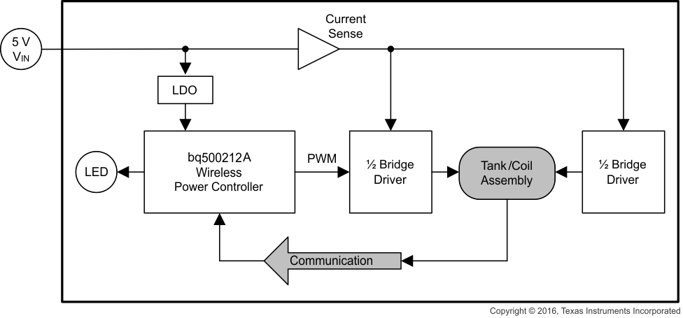
System Diagram

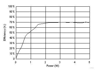
Efficiency vs System Output Power
