SLUSBZ1B October 2014 – March 2017
PRODUCTION DATA.
- 1 Features
- 2 Applications
- 3 Description
- 4 Revision History
- 5 Pin Configuration and Functions
- 6 Specifications
-
7 Detailed Description
- 7.1 Overview
- 7.2 Functional Block Diagram
- 7.3
Feature Description
- 7.3.1 A29 Coil Specification
- 7.3.2 Option Select Pins
- 7.3.3 LED Modes
- 7.3.4 FOD and Parasitic Metal Object Detect (PMOD) Calibration
- 7.3.5 FOD Ping Calibration
- 7.3.6 Shut Down Through External Thermal Sensor or Trigger
- 7.3.7 Fault Handling and Indication
- 7.3.8 Power Transfer Start Signal
- 7.3.9 Power-On Reset
- 7.3.10 External Reset, RESET Pin
- 7.3.11 Trickle Charge and CS100
- 7.4 Device Functional Modes
- 8 Application and Implementation
- 9 Power Supply Recommendations
- 10Layout
- 11Device and Documentation Support
- 12Mechanical, Packaging, and Orderable Information
Package Options
Mechanical Data (Package|Pins)
- RGC|64
Thermal pad, mechanical data (Package|Pins)
- RGC|64
Orderable Information
1 Features
- Qi-Certified WPC v1.2 Solution for 5-W Operation and Proprietary 10-W Charging Capability With TI bq51025 Wireless Power Receiver
- Proprietary Authentication Protocol With TI bq51025 Receiver
- Faster Charging Time
- Compatible With Standard 5-W WPC Receivers
- 12-V Input, Fixed Frequency, Rail Voltage Control Architecture
- Conforms to Wireless Power Consortium (WPC) A29 Transmitter Type Specification
- Enhanced Foreign Objection Detection (FOD) Implementation With FOD Ping that Detects Metal Objects Prior to Power Transfer
- Low Standby Power During Idle and 'Charge Complete'
- 10 Configurable LED Modes Indicate Charging State and Fault Status
- Digital Demodulation Reduces Components and Simplifies Circuitry
2 Applications
- WPC v1.2 Wireless Chargers:
- Qi-Certified Smart Phones, Tablets, and Other Handhelds
- Point-of-Sale Devices
- Custom Wireless Power Applications
- See www.ti.com/wirelesspower for More Information on TI's Wireless Charging Solutions
3 Description
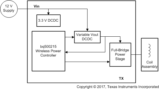
The bq500215 is a dedicated wireless power digital controller that integrates the logic functions required to control wireless power transfer to a single WPC-compliant receiver. The bq500215 complies with the WPC v1.2 standard for power delivery up to 5 W and uses a proprietary bidirectional communication protocol to allow charging at up to 10 W with the bq51025 wireless power receiver. The bq500215 is an intelligent device that periodically pings the surrounding environment for available devices to be powered, detects if a foreign metal object is present on the charging pad, monitors all communication from the device being wirelessly powered, and adjusts power applied to the transmitter coil per feedback received from the powered device. The bq500215 also manages the fault conditions associated with the power transfer and controls the operating mode status indicator. The bq500215 uses a rail voltage control scheme instead of the traditional frequency control to adjust the amount of power delivered to the receiver.
Device Information(1)
| PART NUMBER | PACKAGE | BODY SIZE (NOM) |
|---|---|---|
| bq500215 | VQFN (64) | 9.00 mm × 9.00 mm |
- For all available packages, see the orderable addendum at the end of the data sheet.
Simplified Diagram

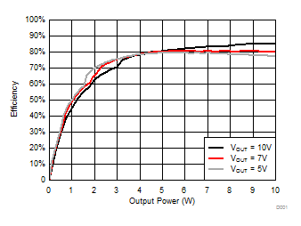
Efficiency vs System Output Power With bq51025 Receiver
