SNLS045C July 1999 – July 2016 DS90LV048A
PRODUCTION DATA.
- 1 Features
- 2 Applications
- 3 Description
- 4 Revision History
- 5 Pin Configuration and Functions
- 6 Specifications
- 7 Parameter Measurement Information
- 8 Detailed Description
- 9 Application and Implementation
- 10Power Supply Recommendations
- 11Layout
- 12Device and Documentation Support
- 13Mechanical, Packaging, and Orderable Information
Package Options
Mechanical Data (Package|Pins)
Thermal pad, mechanical data (Package|Pins)
Orderable Information
1 Features
- > 400-Mbps (200-MHz) Switching Rates
- Flow-Through Pinout Simplifies PCB Layout
- 150-ps Channel-to-Channel Skew (Typical)
- 100-ps Differential Skew (Typical)
- 2.7-ns Maximum Propagation Delay
- 3.3-V Power Supply Design
- High Impedance LVDS Inputs on Power Down
- Low Power Design (40 mW at 3.3-V Static)
- Interoperable With Existing 5-V LVDS Drivers
- Accepts Small Swing (350 mV Typical) Differential Signal Levels
- Supports Input Failsafe
- Open, Short, and Terminated
- 0 V to −100 mV Threshold Region
- Conforms to ANSI/TIA/EIA-644 Standard
- Operating Temperature Range: –40°C to +85°C
- Available in SOIC and TSSOP Package
2 Applications
- Multifunction Printers
- LVDS - LVCMOS Translation
3 Description
The DS90LV048A device is a quad CMOS flow-through differential line receiver designed for applications requiring ultra-low power dissipation and high data rates. The device is designed to support data rates in excess of 400 Mbps (200 MHz) using Low Voltage Differential Signaling (LVDS) technology.
The DS90LV048A accepts low voltage (350 mV typical) differential input signals and translates them to 3-V CMOS output levels. The receiver supports a TRI-STATE function that may be used to multiplex outputs. The receiver also supports open, shorted, and terminated (100-Ω) input fail-safe. The receiver output is HIGH for all fail-safe conditions. The DS90LV048A has a flow-through pinout for easy PCB layout.
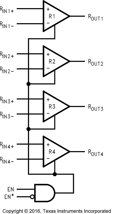
The EN and EN* inputs are ANDed together and control the TRI-STATE outputs. The enables are common to all four receivers. The DS90LV048A and companion LVDS line driver (for example, DS90LV047A) provide a new alternative to high-power PECL/ECL devices for high-speed point-to-point interface applications.
Device Information(1)
| PART NUMBER | PACKAGE | BODY SIZE (NOM) |
|---|---|---|
| DS90LV048A | SOIC (16) | 9.90 mm × 3.91 mm |
| TSSOP (16) | 5.00 mm × 4.40 mm |
- For all available packages, see the orderable addendum at the end of the data sheet.
Functional Diagram
