SBOS374E November 2006 – September 2017 INA200 , INA201 , INA202
PRODUCTION DATA.
- 1 Features
- 2 Applications
- 3 Description
- 4 Revision History
- 5 Pin Configuration and Functions
- 6 Specifications
- 7 Detailed Description
- 8 Application and Implementation
- 9 Power Supply Recommendations
- 10Layout
- 11Device and Documentation Support
- 12Mechanical, Packaging, and Orderable Information
Package Options
Mechanical Data (Package|Pins)
Thermal pad, mechanical data (Package|Pins)
Orderable Information
1 Features
- Complete Current Sense Solution
- Three Gain Options Available:
- INA200 = 20 V/V
- INA201 = 50 V/V
- INA202 = 100 V/V
- 0.6-V Internal Voltage Reference
- Internal Open-Drain Comparator
- Latching Capability on Comparator
- Common-Mode Range: –16 V to 80 V
- High Accuracy: 3.5% Maximum Error Over Temperature
- Bandwidth: 500 kHz (INA200)
- Quiescent Current: 1800 μA (Maximum)
- Packages: SOIC-8, VSSOP-8
2 Applications
- Notebook Computers
- Cell Phones
- Telecom Equipment
- Automotive
- Power Management
- Battery Chargers
- Welding Equipment
3 Description
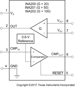
The INA200, INA201, and INA202 devices are high-side current-shunt monitors with voltage output and integrated comparator. The INA20x devices can sense drops across shunts at common-mode voltages from –16 V to 80 V. The INA20x series is available with three output voltage scales: 20 V/V, 50 V/V, and 100 V/V, with a bandwidth up to 500-kHz.
The INA200, INA201, and INA202 devices incorporate an open-drain comparator and internal reference providing a 0.6-V threshold. External dividers set the current trip point. The comparator includes a latching capability, that can be made transparent by grounding (or leaving open) the RESET pin.
The INA200, INA201, and INA202 devices operate from a single 2.7-V to 18-V supply, drawing a maximum of 1800 μA of supply current. Package options include the very small VSSOP-8 and the
SOIC-8. All versions are specified over the extended operating temperature range of –40°C to +125°C.
Device Information(1)
| PART NUMBER | PACKAGE | BODY SIZE (NOM) |
|---|---|---|
| INA200 INA201 INA202 |
SOIC (8) | 4.90 mm × 3.91 mm |
| VSSOP (8) | 3.00 mm × 3.00 mm |
- For all available packages, see the orderable addendum at the end of the data sheet.
Simplified Schematic
