SLLSER6 December 2015 ISO7310-Q1
PRODUCTION DATA.
- 1 Features
- 2 Applications
- 3 Description
- 4 Revision History
- 5 Pin Configuration and Functions
-
6 Specifications
- 6.1 Absolute Maximum Ratings
- 6.2 ESD Ratings
- 6.3 Recommended Operating Conditions
- 6.4 Thermal Information
- 6.5 Electrical Characteristics—5-V Supply
- 6.6 Supply Current Characteristics—5-V Supply
- 6.7 Electrical Characteristics—3.3-V Supply
- 6.8 Supply Current Characteristics—3.3-V Supply
- 6.9 Power Dissipation Characteristics
- 6.10 Switching Characteristics—5-V Supply
- 6.11 Switching Characteristics
- 6.12 Typical Characteristics
- 7 Parameter Measurement Information
- 8 Detailed Description
- 9 Applications and Implementation
- 10Power Supply Recommendations
- 11Layout
- 12Device and Documentation Support
- 13Mechanical, Packaging, and Orderable Information
Package Options
Refer to the PDF data sheet for device specific package drawings
Mechanical Data (Package|Pins)
- D|8
Thermal pad, mechanical data (Package|Pins)
Orderable Information
1 Features
- Qualified for Automotive Applications
- AEC-Q100 Qualified With the Following Results:
- Device Temperature Grade 1: –40°C to +125°C Ambient Operating Temperature Range
- Device HBM Classification Level 3A
- Device CDM Classification Level C6
- Signaling Rate: 25 Mbps
- Integrated Noise Filter at the Input
- Default Output High and Low Options
- Low Power Consumption: Typical ICC
- 1.9 mA at 1 Mbps, 3.8 mA at 25 Mbps (5-V Supplies)
- 1.4 mA at 1 Mbps, 2.6 mA at 25 Mbps (3.3-V Supplies)
- Low Propagation Delay: 32 ns Typical (5-V Supplies)
- 65-kV/μs Transient Immunity, Typical (5-V Supplies)
- Robust Electromagnetic Compatibility (EMC)
- System-level ESD, EFT, and Surge Immunity
- Low Emissions
- Isolation Barrier Life: > 25 Years
- Operates from 3.3-V and 5-V Supplies
- 3.3-V and 5-V Level Translation
- Narrow Body SOIC-8 Package
- Safety and Regulatory Approvals:
- 4242-VPK Isolation per DIN V VDE V 0884-10 and DIN EN 61010-1
- 3000-VRMS Isolation for 1 minute per UL 1577
- CSA Component Acceptance Notice 5A,
IEC 60950-1 and IEC 61010-1 End Equipment Standards - Planned CQC Certification per GB4943.1-2011
2 Applications
- Opto-Coupler Replacement in:
- Industrial FieldBus
- ProfiBus
- ModBus
- DeviceNet™ Data Buses
- Servo Control Interface
- Motor Control
- Power Supplies
- Battery Packs
- Industrial FieldBus
3 Description
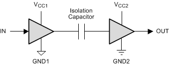
The ISO7310-Q1 device provides galvanic isolation up to 3000 VRMS for 1 minute per UL 1577 and 4242 VPK per VDE V 0884-10. These devices have one isolated channel comprised of a logic input and output buffer separated by a silicon dioxide (SiO2) insulation barrier. Used in conjunction with isolated power supplies, the ISO7310-Q1 device prevents noise currents on a data bus or other circuit from entering the local ground and interfering with or damaging sensitive circuitry. The device has integrated noise filters for harsh industrial environment where short noise pulses may be present at the device input pins.
The ISO7310-Q1 device has TTL input thresholds and operate from 3-V to 5.5-V supply levels. Through innovative chip design and layout techniques, electromagnetic compatibility of the ISO7310-Q1 device has been significantly enhanced to enable system-level ESD, EFT, Surge and Emissions compliance.
Device Information(1)
| PART NUMBER | PACKAGE | BODY SIZE (NOM) |
|---|---|---|
| ISO7310-Q1 | SOIC (8) | 4.90 mm × 3.91 mm |
- For all available packages, see the orderable addendum at the end of the datasheet.
Simplified Schematic

4 Revision History
| DATE | REVISION | NOTES |
|---|---|---|
| December 2015 | * | Initial release. |