SNOI146C September 2011 – December 2017 ADC141S628-Q1
PRODUCTION DATA.
- 1 Features
- 2 Applications
- 3 Description
- 4 Revision History
- 5 Pin Configuration and Functions
- 6 Specifications
- 7 Detailed Description
- 8 Application and Implementation
- 9 Power Supply Recommendations
- 10Layout
- 11Device and Documentation Support
- 12Mechanical, Packaging, and Orderable Information
パッケージ・オプション
デバイスごとのパッケージ図は、PDF版データシートをご参照ください。
メカニカル・データ(パッケージ|ピン)
- DGS|10
サーマルパッド・メカニカル・データ
発注情報
8 Application and Implementation
NOTE
Information in the following applications sections is not part of the TI component specification, and TI does not warrant its accuracy or completeness. TI’s customers are responsible for determining suitability of components for their purposes. Customers should validate and test their design implementation to confirm system functionality.
8.1 Application Information
8.1.1 Application Circuits
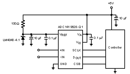
The following figure is an example of the ADC141S628-Q1 in a typical application circuit. This circuit is basic and generally requires modification for specific circumstances.
8.1.1.1 Data Acquisition
Figure 35 shows a typical connection diagram for the ADC141S628-Q1 operating at VA of 5 V. VREF is connected to a 4.1-V shunt reference, the LM4040-4.1, to define the analog input range of the ADC141S628-Q1 independent of supply variation on the 5-V supply line. Decouple the VREF pin to the ground plane by a 0.1-µF ceramic capacitor and a tantalum capacitor of 10 µF. The 0.1-µF capacitor must be placed as close as possible to the VREF pin while the placement of the tantalum capacitor is less critical. The VA and VIO pins of the ADC141S628-Q1 are also recommended to be decoupled to ground by a 0.1-µF ceramic capacitor in parallel with a 10-µF tantalum capacitor.
 Figure 35. Low-Cost, Low-Power Data Acquisition System