JAJSI32 October   2019 ADS1235-Q1

PRODUCTION DATA.  

  1. 特長
  2. アプリケーション
  3. 概要
    1.     Device Images
      1.      ブロック図
      2.      ADC変換ノイズ
  4. 改訂履歴
  5. 概要(続き)
  6. Pin Configuration and Functions
    1.     Pin Functions
  7. Specifications
    1. 7.1 Absolute Maximum Ratings
    2. 7.2 ESD Ratings
    3. 7.3 Recommended Operating Conditions
    4. 7.4 Thermal Information
    5. 7.5 Electrical Characteristics
    6. 7.6 Timing Requirements
    7. 7.7 Switching Characteristics
    8. 7.8 Typical Characteristics
  8. Parameter Measurement Information
    1. 8.1 Noise Performance
  9. Detailed Description
    1. 9.1 Overview
    2. 9.2 Functional Block Diagram
    3. 9.3 Feature Description
      1. 9.3.1 Analog Inputs
        1. 9.3.1.1 ESD Diodes
        2. 9.3.1.2 Input Multiplexer
        3. 9.3.1.3 Temperature Sensor
        4. 9.3.1.4 Inputs Open
        5. 9.3.1.5 Internal VCOM Connection
        6. 9.3.1.6 Alternate Functions
      2. 9.3.2 PGA
        1. 9.3.2.1 Input Voltage Range
        2. 9.3.2.2 PGA Bypass Mode
      3. 9.3.3 PGA Voltage Monitor
      4. 9.3.4 Reference Voltage
        1. 9.3.4.1 External Reference
        2. 9.3.4.2 AVDD – AVSS Reference (Default)
        3. 9.3.4.3 Reference Monitor
      5. 9.3.5 General-Purpose Input/Outputs (GPIOs)
      6. 9.3.6 Modulator
      7. 9.3.7 Digital Filter
        1. 9.3.7.1 Sinc Filter
          1. 9.3.7.1.1 Sinc Filter Frequency Response
        2. 9.3.7.2 FIR Filter
          1. 9.3.7.2.1 FIR Filter Frequency Response
        3. 9.3.7.3 Filter Bandwidth
        4. 9.3.7.4 50-Hz and 60-Hz Normal Mode Rejection
    4. 9.4 Device Functional Modes
      1. 9.4.1 Conversion Control
        1. 9.4.1.1 Continuous-Conversion Mode
        2. 9.4.1.2 Pulse-Conversion Mode
        3. 9.4.1.3 Conversion Latency
        4. 9.4.1.4 Start-Conversion Delay
      2. 9.4.2 Chop Mode
      3. 9.4.3 AC-Bridge Excitation Mode
      4. 9.4.4 ADC Clock Mode
      5. 9.4.5 Power-Down Mode
        1. 9.4.5.1 Hardware Power-Down
        2. 9.4.5.2 Software Power-Down
      6. 9.4.6 Reset
        1. 9.4.6.1 Power-on Reset
        2. 9.4.6.2 Reset by Pin
        3. 9.4.6.3 Reset by Command
      7. 9.4.7 Calibration
        1. 9.4.7.1 Offset and Full-Scale Calibration
          1. 9.4.7.1.1 Offset Calibration Registers
          2. 9.4.7.1.2 Full-Scale Calibration Registers
        2. 9.4.7.2 Offset Self-Calibration (SFOCAL)
        3. 9.4.7.3 Offset System-Calibration (SYOCAL)
        4. 9.4.7.4 Full-Scale Calibration (GANCAL)
        5. 9.4.7.5 Calibration Command Procedure
        6. 9.4.7.6 User Calibration Procedure
    5. 9.5 Programming
      1. 9.5.1 Serial Interface
        1. 9.5.1.1 Chip Select (CS)
        2. 9.5.1.2 Serial Clock (SCLK)
        3. 9.5.1.3 Data Input (DIN)
        4. 9.5.1.4 Data Output/Data Ready (DOUT/DRDY)
        5. 9.5.1.5 Serial Interface Auto-Reset
      2. 9.5.2 Data Ready (DRDY)
        1. 9.5.2.1 DRDY in Continuous-Conversion Mode
        2. 9.5.2.2 DRDY in Pulse-Conversion Mode
        3. 9.5.2.3 Data Ready by Software Polling
      3. 9.5.3 Conversion Data
        1. 9.5.3.1 Status byte (STATUS)
        2. 9.5.3.2 Conversion Data Format
      4. 9.5.4 CRC
      5. 9.5.5 Commands
        1. 9.5.5.1  NOP Command
        2. 9.5.5.2  RESET Command
        3. 9.5.5.3  START Command
        4. 9.5.5.4  STOP Command
        5. 9.5.5.5  RDATA Command
        6. 9.5.5.6  SYOCAL Command
        7. 9.5.5.7  GANCAL Command
        8. 9.5.5.8  SFOCAL Command
        9. 9.5.5.9  RREG Command
        10. 9.5.5.10 WREG Command
        11. 9.5.5.11 LOCK Command
        12. 9.5.5.12 UNLOCK Command
    6. 9.6 Register Map
      1. 9.6.1  Device Identification (ID) Register (address = 00h) [reset = Cxh]
        1. Table 28. ID Register Field Descriptions
      2. 9.6.2  Device Status (STATUS) Register (address = 01h) [reset = 01h]
        1. Table 29. STATUS Register Field Descriptions
      3. 9.6.3  Mode 0 (MODE0) Register (address = 02h) [reset = 24h]
        1. Table 30. MODE0 Register Field Descriptions
      4. 9.6.4  Mode 1 (MODE1) Register (address = 03h) [reset = 01h]
        1. Table 31. MODE1 Register Field Descriptions
      5. 9.6.5  Mode 2 (MODE2) Register (address = 04h) [reset = 00h]
        1. Table 32. MODE2 Register Field Descriptions
      6. 9.6.6  Mode 3 (MODE3) Register (address = 05h) [reset = 00h]
        1. Table 33. MODE3 Register Field Descriptions
      7. 9.6.7  Reference Configuration (REF) Register (address = 06h) [reset = 05h]
        1. Table 34. REF Register Field Descriptions
      8. 9.6.8  Offset Calibration (OFCALx) Registers (address = 07h, 08h, 09h) [reset = 00h, 00h, 00h]
        1. Table 35. OFCAL0, OFCAL1, OFCAL2 Registers Field Description
      9. 9.6.9  Full-Scale Calibration (FSCALx) Registers (address = 0Ah, 0Bh, 0Ch) [reset = 00h, 00h, 40h]
        1. Table 36. FSCAL0, FSCAL1, FSCAL2 Registers Field Description
      10. 9.6.10 Reserved (RESERVED) Register (address = 0Dh) [reset = FFh]
        1. Table 37. RESERVED Register Field Descriptions
      11. 9.6.11 Reserved (RESERVED) Register (address = 0Eh) [reset = 00h]
        1. Table 38. RESERVED Register Field Descriptions
      12. 9.6.12 Reserved (RESERVED) Register (address = 0Fh) [reset = 00h]
        1. Table 39. RESERVED Register Field Descriptions
      13. 9.6.13 PGA Configuration (PGA) Register (address = 10h) [reset = 00h]
        1. Table 40. PGA Register Field Descriptions
      14. 9.6.14 Input Multiplexer (INPMUX) Register (address = 11h) [reset = FFh]
        1. Table 41. INPMUX Register Field Descriptions
  10. 10Application and Implementation
    1. 10.1 Application Information
      1. 10.1.1 Input Range
      2. 10.1.2 Input Overload
      3. 10.1.3 Unused Inputs and Outputs
      4. 10.1.4 Multiplexed 2-Bridge Input Example
      5. 10.1.5 AC-Bridge Excitation Example
      6. 10.1.6 Serial Interface and Digital Connections
    2. 10.2 Typical Application
      1. 10.2.1 Design Requirements
      2. 10.2.2 Detailed Design Procedure
      3. 10.2.3 Application Curves
    3. 10.3 Initialization Setup
  11. 11Power Supply Recommendations
    1. 11.1 Power-Supply Decoupling
    2. 11.2 Analog Power-Supply Clamp
    3. 11.3 Power-Supply Sequencing
  12. 12Layout
    1. 12.1 Layout Guidelines
    2. 12.2 Layout Example
  13. 13デバイスおよびドキュメントのサポート
    1. 13.1 ドキュメントのサポート
      1. 13.1.1 関連資料
    2. 13.2 ドキュメントの更新通知を受け取る方法
    3. 13.3 コミュニティ・リソース
    4. 13.4 商標
    5. 13.5 静電気放電に関する注意事項
    6. 13.6 Glossary
  14. 14メカニカル、パッケージ、および注文情報

パッケージ・オプション

メカニカル・データ(パッケージ|ピン)
サーマルパッド・メカニカル・データ
発注情報

Sinc Filter Frequency Response

The overall frequency response of the sinc filter is low pass. The filter reduces signal and noise beginning at the -3-dB bandwidth. Changing the data rate and filter order changes the filter bandwidth together with the rate of frequency roll-off. See the Filter Bandwidth section for the bandwidth of the filter settings.

Figure 49 shows the frequency response of the sinc filter at 2400 SPS for various orders of the sinc filter. The peaks and nulls are characteristic of the sinc filter response. The frequency response nulls occur at f (Hz) = N · fDATA, where N = 1, 2, 3 and so on. At the null frequencies, the filter has zero gain. The response nulls are superimposed with the larger nulls beginning at 14400 Hz. The larger nulls are produced by the first stage. The frequency response is similar to that of data rates 2.5 SPS through 7200 SPS. Figure 50 shows the frequency response nulls for 10 SPS.
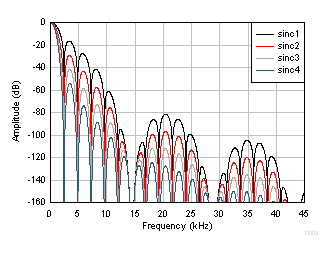
ADS1235-Q1 D103_sbas760.gifFigure 49. Sinc Frequency Response (2400 SPS)
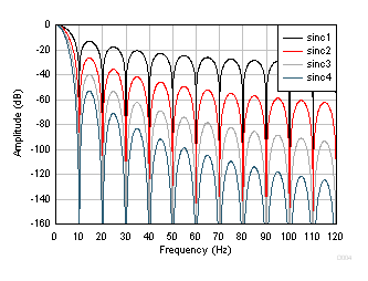
ADS1235-Q1 D104_sbas760.gifFigure 50. Sinc Frequency Response (10 SPS)

Figure 51 and Figure 52 show the frequency response of data rates 50 SPS and 60 SPS, respectively. Increase the attenuation at 50 Hz or 60 Hz and harmonics by increasing the order of the sinc filter, as shown in the figures.
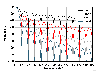
ADS1235-Q1 D105_sbas760.gifFigure 51. Sinc Frequency Response (50 SPS)
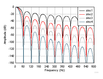
ADS1235-Q1 D106_sbas760.gifFigure 52. Sinc Frequency Response (60 SPS)

Figure 53 and Figure 54 show the detailed frequency response at 50 SPS and 60 SPS, respectively.
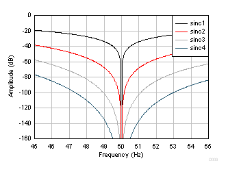
ADS1235-Q1 D109_sbas760.gifFigure 53. Detail Sinc Frequency Response (50 SPS)
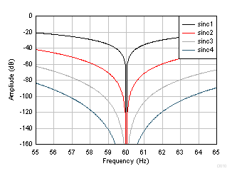
ADS1235-Q1 D110_sbas760.gifFigure 54. Detail Sinc Frequency Response (60 SPS)