JAJSIY6C December 2011 – April 2020 ADS1291 , ADS1292 , ADS1292R
PRODUCTION DATA.
- 1 特長
- 2 アプリケーション
- 3 概要
- 4 改訂履歴
- 5 Pin Configuration and Functions
- 6 Specifications
- 7 Parameter Measurement Information
-
8 Detailed Description
- 8.1 Overview
- 8.2 Functional Block Diagram
- 8.3
Feature Description
- 8.3.1 EMI Filter
- 8.3.2
Input Multiplexer
- 8.3.2.1 Device Noise Measurements
- 8.3.2.2 Test Signals (TestP and TestN)
- 8.3.2.3 Auxiliary Differential Input (RESP_MODN/IN3N, RESP_MODN/IN3P)
- 8.3.2.4 Temperature Sensor (TEMPP, TEMPN)
- 8.3.2.5 Supply Measurements (MVDDP, MVDDN)
- 8.3.2.6 Lead-Off Excitation Signals (LoffP, LoffN)
- 8.3.2.7 Auxiliary Single-Ended Input
- 8.3.3 Analog Input
- 8.3.4 PGA Settings and Input Range
- 8.3.5 Digital Decimation Filter
- 8.3.6 Reference
- 8.3.7 Clock
- 8.3.8 Data Format
- 8.3.9 Multiple Device Configuration
- 8.3.10 ECG-Specific Functions
- 8.3.11 Setting the Device for Basic Data Capture
- 8.4 Device Functional Modes
- 8.5
Programming
- 8.5.1 SPI Interface
- 8.5.2
SPI Command Definitions
- 8.5.2.1 WAKEUP: Exit STANDBY Mode
- 8.5.2.2 STANDBY: Enter STANDBY Mode
- 8.5.2.3 RESET: Reset Registers to Default Values
- 8.5.2.4 START: Start Conversions
- 8.5.2.5 STOP: Stop Conversions
- 8.5.2.6 OFFSETCAL: Channel Offset Calibration
- 8.5.2.7 RDATAC: Read Data Continuous
- 8.5.2.8 SDATAC: Stop Read Data Continuous
- 8.5.2.9 RDATA: Read Data
- 8.5.2.10 Sending Multi-Byte Commands
- 8.5.2.11 RREG: Read From Register
- 8.5.2.12 WREG: Write to Register
- 8.6
Register Maps
- 8.6.1
User Register Description
- 8.6.1.1 ID: ID Control Register (Factory-Programmed, Read-Only) (address = 00h)
- 8.6.1.2 CONFIG1: Configuration Register 1 (address = 01h)
- 8.6.1.3 CONFIG2: Configuration Register 2 (address = 02h)
- 8.6.1.4 LOFF: Lead-Off Control Register (address = 03h)
- 8.6.1.5 CH1SET: Channel 1 Settings (address = 04h)
- 8.6.1.6 CH2SET: Channel 2 Settings (address = 05h)
- 8.6.1.7 RLD_SENS: Right Leg Drive Sense Selection (address = 06h)
- 8.6.1.8 LOFF_SENS: Lead-Off Sense Selection (address = 07h)
- 8.6.1.9 LOFF_STAT: Lead-Off Status (address = 08h)
- 8.6.1.10 RESP1: Respiration Control Register 1 (address = 09h)
- 8.6.1.11 RESP2: Respiration Control Register 2 (address = 0Ah)
- 8.6.1.12 GPIO: General-Purpose I/O Register (address = 0Bh)
- 8.6.1
User Register Description
- 9 Application and Implementation
- 10Power Supply Recommendations
- 11Layout
- 12デバイスおよびドキュメントのサポート
- 13メカニカル、パッケージ、および注文情報
パッケージ・オプション
メカニカル・データ(パッケージ|ピン)
サーマルパッド・メカニカル・データ
- PBS|32
発注情報
8.3.10.2.3 RLD Lead-Off
The ADS1291, ADS1292, and ADS1292R provide two modes for determining whether the RLD is correctly connected:
- RLD lead-off detection during normal operation
- RLD lead-off detection during power-up
The following sections provide details of the two modes of operation.
RLD Lead-Off Detection During Normal Operation
During normal operation, the ADS1291, ADS1292, and ADS1292R RLD lead-off at power-up function cannot be used because it is necessary to power off the RLD amplifier.
RLD Lead-Off Detection At Power-Up
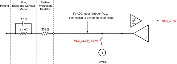
This feature is included in the ADS1291, ADS1292, and ADS1292R for use in determining whether the right leg electrode is suitably connected. At power-up, the ADS1291, ADS1292, and ADS1292R provides a procedure to determine the RLD electrode connection status using a current sink, as shown in Figure 39. The reference level of the comparator is set to determine the acceptable RLD impedance threshold.

NOTE:
The RP value must be selected in order to be below the maximum allowable current flow into a patient (in accordance with the relevant specification the latest revision of IEC 60601).When the RLD amplifier is powered on, the current source has no function. Only the comparator can be used to sense the voltage at the output of the RLD amplifier. The comparator thresholds are set by the same LOFF[7:5] bits used to set the thresholds for other negative inputs.