JAJS454C January 2010 – September 2017 ADS7924
PRODUCTION DATA.
- 1 特長
- 2 アプリケーション
- 3 概要
- 4 改訂履歴
- 5 Pin Configuration and Functions
- 6 Specifications
- 7 Detailed Description
-
8 Application and Implementation
- 8.1
Application Information
- 8.1.1 Using an Operational Amplifier Between Multiplexer Output and ADC Input
- 8.1.2 Using an Operational Amplifier and RC Filter Between Multiplexer Output and ADC Input
- 8.1.3 Using an RC Filter Between Multiplexer Output and ADC Input
- 8.1.4 Operational Amplifier With Filter and Gain Option Between Multiplexer Output and ADC Input
- 8.1.5 Driving an RC Filter With an Operational Amplifier Between Multiplexer Output and ADC Input
- 8.1.6 Average Power Consumption
- 8.2 Typical Application
- 8.1
Application Information
- 9 Power Supply Recommendations
- 10Layout
- 11デバイスおよびドキュメントのサポート
- 12メカニカル、パッケージ、および注文情報
パッケージ・オプション
メカニカル・データ(パッケージ|ピン)
- RTE|16
サーマルパッド・メカニカル・データ
- RTE|16
発注情報
8 Application and Implementation
NOTE
Information in the following applications sections is not part of the TI component specification, and TI does not warrant its accuracy or completeness. TI’s customers are responsible for determining suitability of components for their purposes. Customers should validate and test their design implementation to confirm system functionality.
8.1 Application Information
The ADS7924 device provides a break-out point in the signal path between the multiplexer output and the ADC input for external signal conditioning, if desired. Typical uses include adding an operational amplifier, such as the TLV2780, along with an RC filter circuit. Different application circuits are described in following sections.
8.1.1 Using an Operational Amplifier Between Multiplexer Output and ADC Input
Adding an operational amplifier provides a high input impedance to the sensor source and buffers the capacitive ADC input from high-impedance sensor circuits, as shown in Figure 57. High-impedance input signals can be momentarily disrupted when coupled directly to a capacitive input like that of a sampling ADC. This disruption can create errors when sampling. The use of an operational amplifier is recommended in these cases.
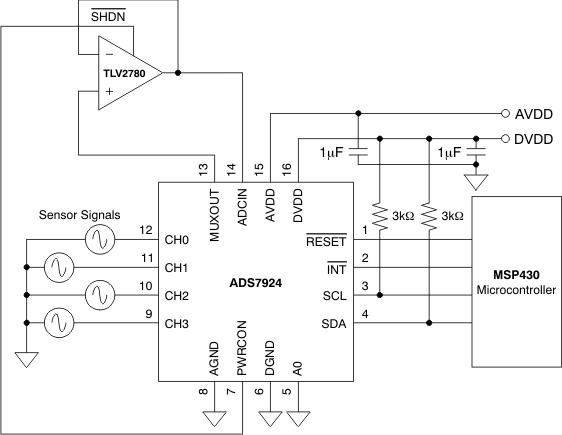 Figure 57. Sensor Data Acquisition With TLV2780 Buffer Amplifier
8.1.2 Using an Operational Amplifier and RC Filter Between Multiplexer Output and ADC Input
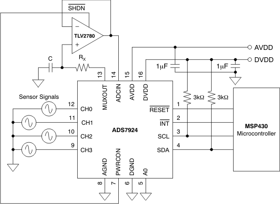
Placing an RC low-pass filter in the signal path allows for filtering out noise. The RC component values should allow for sufficient settling time when changing from channel to channel. The time required for a full-scale input signal to settle to within 1LSB of a 12-bit ADC is given by Equation 3:
RX and C form a low-pass filter for removing sensor and noise from other sources at the operational amplifier input pin. The low-pass bandwidth is given by Equation 4:
The f–3dB should be chosen so that the signals of interest are within half of the programmable sampling frequency. The noise bandwidth is given by Equation 5:
This term should be set to reduce noise bandwidth but still allow for enough settling time. The ADS7924 has internal registers ACQCONFIG (address = 14h), PWRCONF (address = 15h), and SLPCONFIG (address = 13h) that can be programmed to slow down the channel-to-channel power up, acquisition, and sleep periods if needed to allow for a longer settling time requirement.
In Figure 58, R is the sum of the sensor output impedance RSENSOR, the internal MUX resistance RMUX (approximately 60 Ω), and external resistor RX. The primary benefit of having the filter at the input of the operational amplifier is that the amplifier does not have to drive the filter, which can cause instability with large capacitor values that may be needed to filter noise to low levels.
The TLV2780 typically powers up from a shutdown state in 800 ns. This period is well within the ADS7924 minimum acquisition time of 6μs. Setting the PWRCONFIG register (address = 15h) allows for more time if another operational amplifier with a shutdown feature is used.
8.1.3 Using an RC Filter Between Multiplexer Output and ADC Input
For applications where low-output impedance signals are provided for the ADS7924 inputs, a simple RC filter may suffice, as shown in Figure 59.
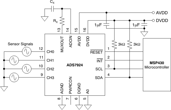
CX should be greater than 200 pF, if possible. When coupled directly to the ADC input, using a capacitor with this value allows for faster settling when scanning between channels.
8.1.4 Operational Amplifier With Filter and Gain Option Between Multiplexer Output and ADC Input
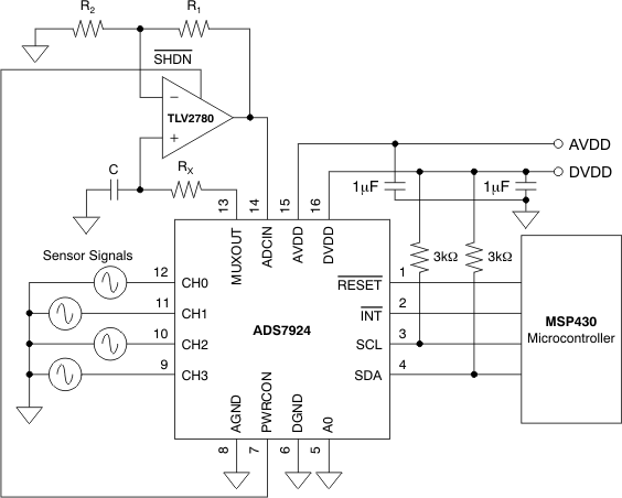
Both filtering and gain are added in Figure 60. Gain is given by Equation 6:
where
- R is the sum of the sensor output impedance RSENSOR, the internal MUX resistance RMUX (approximately 60 Ω), and the external resistor RX.
NOTE:
f–3dB BW = 159 kHz, R = 1 kΩ, and C = 1 nF where R = RMUX + RSENSOR + RX, and RMUX is approximately 60 Ω. Gain = 1 + R1 / R2.8.1.5 Driving an RC Filter With an Operational Amplifier Between Multiplexer Output and ADC Input
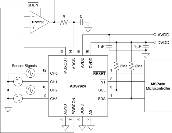
A filter can be placed at the output of the operational amplifier, as shown in Figure 61. Ensure that the operational amplifier is capable of driving the RC filter circuit without the operational amplifier becoming unstable. One of the benefits of this circuit is that the operational amplifier noise is filtered along with sensor and other system noise right at the ADC input pin.
NOTE:
C = 200 pF, R = 1 kΩ, and the capacitance at the ADCIN pin is approximately 15 pF.8.1.6 Average Power Consumption
With its fast conversion time and programmable sleep time with near-zero power, the ADS7924 allows periodic monitoring of the inputs with a very low average power dissipation, especially as the monitoring interval increases. The average current required can be calculated as the weighed average of the currents consumed during the power up, acquisition, converting, and sleep periods using Equation 7.

As an example, calculate the average current in the following configuration:
- Mode programmed to Auto-Scan with Sleep
- Power-up time (tPU) programmed to '0'
- Acquisition time (tACQ) programmed to 6 μs
- Sleep time (tSLEEP) programmed to 2.5 ms
- AVDD = 2.2 V
Looking at Figure 27, the cycle time is seen to equal tCYCLE = 4tPU + 4tACQ + 4tCONV + 4tSLEEP = 4(0) + 4(6 μs) + 4(4 μs) + 4(2.5 ms) = 10.04 ms.
Table 5 lists the supply current for different supply voltages and operating conditions. Using the data for 2.2 V with the calculated cycle time in Equation 7 gives the following average current:

Table 5. Supply Current for Various Operating Conditions
| STATUS | AVDD | |||
|---|---|---|---|---|
| 5 V | 3.3 V | 2.7 V | 2.2 V | |
| Idle | 1 µA | 1 µA | 1 µA | 1 µA |
| Awake | 45 µA | 25 µA | 20 µA | 15 µA |
| Acquiring | 315 µA | 285 µA | 275 µA | 270 µA |
| Converting | 730 µA | 520 µA | 450 µA | 400 µA |
| Sleeping | 3 µA | 2 µA | 1.5 µA | 1.25 µA |
The acquisition, conversion, and sleep times are multiplied by 4 because these are repeated four times in one cycle when in auto-scan with sleep mode.
Average power dissipation for the previous configuration where all four inputs are monitored every 10 ms is (2.2 V)(2.5 μA) = 5.5 μW.
Figure 3 and Figure 4 plot Equation 7 to help illustrate the relationship between cycle time and average power dissipation.
8.2 Typical Application
Figure 62 shows a 0-V to 10-V Input DAQ Circuit with a DC accuracy of 0.1%.
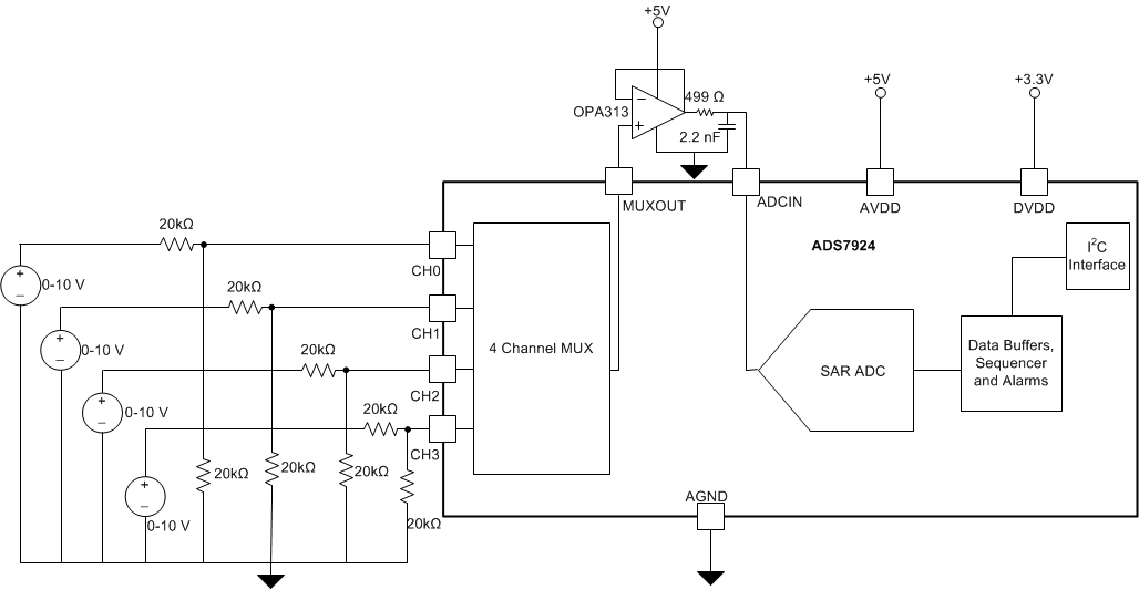 Figure 62. 0-V to 10-V Input DAQ Circuit
8.2.1 Design Requirements
Table 6 shows the design parameters for this typical application.
Table 6. Design Parameters
| DESIGN PARAMETER | DESIGN GOAL |
|---|---|
| Throughput | 100 SPS |
| DC Accuracy | 0.1% |
| Full Scale Step Settling | 20 µs |
| DC Noise at input of ADC | 200 µV RMS |
| Input Impedance | 40 kΩ |
8.2.2 Detailed Design Procedure
8.2.2.1 Setting the Throughput
The throughput was set by selecting a sleep time of 40 ms, sleep divider of 4 and acquisition time of 6 µs.
8.2.2.2 Selecting the Operational Amplifier
The key parameters for selecting the operational amplifier for this circuit are noise, offset voltage and input bias current. The offset voltage and input bias current affect the DC accuracy whereas the noise of the amplifier increases the total noise at the input of ADC, the total noise at the input of ADC (Vn) can be calculated by Equation 9. Vn must be less than 200-µV RMS for this circuit design.

where
- en_RMS is the input voltage noise density of the amplifier.
- VN_ADC is the DC noise of the ADC. For ADS7924 , DC Noise is specified as 0.125 LSB RMS.
- V 1/f_AMP_PP is the peak to peak low-frequency noise at the input of amplifier.
- f-3dB is the bandwidth of RC filter at the output of amplifier.
OPA313 is selected for this design for its low noise (25 nv/√Hz), low offset voltage (0.5 mV) and low input bias current (0.2 pA).
8.2.2.3 Selecting the RC Filter
The RC filter at the output of amplifier affect full scale settling time and noise at the input of ADC. Full scale settling time can be calculated using Equation 3 and the noise at input of ADC can be calculated using Equation 9. A value of 499 Ω and 2.2 nF is used for achieving the full scale settling time of 20 µs and total DC noise of less than 200 µV RMS.
8.2.3 Application Curves
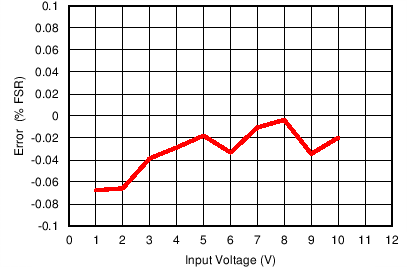
| Max Error = -0.0035% | Min Error = -0.067% | |
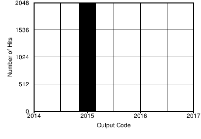
| Sigma = 0.05 | Noise = 61µV RMS |