SBAS652A May 2014 – August 2014 ADS7950-Q1 , ADS7951-Q1 , ADS7952-Q1 , ADS7953-Q1 , ADS7954-Q1 , ADS7956-Q1 , ADS7957-Q1 , ADS7958-Q1 , ADS7959-Q1 , ADS7960-Q1 , ADS7961-Q1
PRODUCTION DATA.
- 1 Features
- 2 Applications
- 3 Description
- 4 Revision History
- 5 Device Comparison Table
- 6 Pin Configurations and Functions
-
7 Specifications
- 7.1 Absolute Maximum Ratings
- 7.2 Handling Ratings
- 7.3 Recommended Operating Conditions
- 7.4 Thermal Information
- 7.5 Electrical Characteristics: ADS7950-Q1, ADS7951-Q1, ADS7952-Q1, ADS7953-Q1
- 7.6 Electrical Characteristics: ADS7954-Q1, ADS7956-Q1, ADS7957-Q1
- 7.7 Electrical Characteristics: ADS7958-Q1, ADS7959-Q1, ADS7960-Q1, ADS7961-Q1
- 7.8 Timing Requirements
- 7.9 Typical Characteristics (All ADS79xx-Q1 Family Devices)
- 7.10 Typical Characteristics (12-Bit Devices Only)
- 8 Detailed Description
- 9 Application and Implementation
- 10Power-Supply Recommendations
- 11Layout
- 12Device and Documentation Support
- 13Mechanical, Packaging, and Orderable Information
7 Specifications
7.1 Absolute Maximum Ratings(1)
over operating free-air temperature range (unless otherwise noted).| MIN | MAX | UNIT | |||
|---|---|---|---|---|---|
| Supply voltage to ground | +VA to AGND, +VBD to BDGND | –0.3 | 7 | V | |
| Signal input | AINP or CHn to AGND | –0.3 | V(+VA) + 0.3 | V | |
| Digital input | To BDGND | –0.3 | 7 | V | |
| Digital output | To BDGND | –0.3 | V(+VA) + 0.3 | V | |
| Junction temperature, TJ | 150 | °C | |||
(1) Stresses beyond those listed as absolute maximum ratings may cause permanent damage to the device. These are stress ratings only, and functional operation of the device at these or any other conditions beyond those indicated as recommended operating conditions is not implied. Exposure to absolute-maximum-rated conditions for extended periods may affect device reliability.
7.2 Handling Ratings
| MIN | MAX | UNIT | ||||
|---|---|---|---|---|---|---|
| Tstg | Storage temperature range | –65 | 150 | °C | ||
| V(ESD) | Electrostatic discharge | Human-body model (HBM), per AEC Q100-002(1), level H2 | –2 | 2 | kV | |
| Charged-device model (CDM), per AEC Q100-001, level C4B | Corner pins (1, 15, 16, and 30 for 30-pin packages 1, 19, 20, and 38 for 38-pin packages) |
–750 | 750 | V | ||
| All pins | –500 | 500 | ||||
(1) AEC Q100-002 indicates HBM stressing is done in accordance with the ANSI/ESDA/JEDEC JS-001 specification.
7.3 Recommended Operating Conditions
over operating free-air temperature range (unless otherwise noted)| MIN | NOM | MAX | UNIT | |||
|---|---|---|---|---|---|---|
| V(+VA) | Analog power-supply voltage | 2.7 | 3.3 | 5.25 | V | |
| V(+VBD) | Digital I/O-supply voltage | 1.7 | 3.3 | V(+VA) | V | |
| V(REF) | Reference voltage | 2 | 2.5 | 3 | V | |
| ƒ(SCLK) | SCLK frequency | 20 | MHz | |||
| TA | Operating temperature range | –40 | 125 | °C | ||
7.4 Thermal Information
| THERMAL METRIC(1) | ADS79xx-Q1 | UNIT | ||
|---|---|---|---|---|
| DBT (TSSOP) | DBT (TSSOP) | |||
| 38 PINS | 30 PINS | |||
| RθJA | Junction-to-ambient thermal resistance | 83.6 | 89.8 | °C/W |
| RθJC(top) | Junction-to-case (top) thermal resistance | 29.8 | 22.9 | |
| RθJB | Junction-to-board thermal resistance | 44.7 | 43.1 | |
| ψJT | Junction-to-top characterization parameter | 2.9 | 0.8 | |
| ψJB | Junction-to-board characterization parameter | 44.1 | 42.5 | |
| RθJC(bot) | Junction-to-case (bottom) thermal resistance | n/a | n/a | |
(1) For more information about traditional and new thermal metrics, see the IC Package Thermal Metrics application report, SPRA953.
7.5 Electrical Characteristics: ADS7950-Q1, ADS7951-Q1, ADS7952-Q1, ADS7953-Q1
V(+VA) = 2.7 V to 5.25 V, V(+VBD) = 1.7 V to V(+VA), Vref = 2.5 V ± 0.1 V, TA = –40°C to 125°C, ƒsample = 1 MHz (unless otherwise noted)| PARAMETER | TEST CONDITIONS | MIN | TYP | MAX | UNIT | ||
|---|---|---|---|---|---|---|---|
| ANALOG INPUT | |||||||
| Full-scale input span(1) | Range 1 | 0 | Vref | V | |||
| Range 2 while 2 × Vref ≤ +VA | 0 | 2 × Vref | V | ||||
| Absolute input range | Range 1 | –0.2 | Vref + 0.2 | V | |||
| Range 2 while 2 × Vref ≤ +VA | –0.2 | 2 × Vref + 0.2 | V | ||||
| Input capacitance | 15 | ρF | |||||
| Input leakage current | TA = 125°C | 61 | nA | ||||
| SYSTEM PERFORMANCE | |||||||
| Resolution | 12 | Bits | |||||
| No missing codes | 11 | Bits | |||||
| Integral linearity | –1.5 | ±0.75 | 1.5 | LSB(2) | |||
| Differential linearity | –2 | ±0.75 | 1.5 | LSB | |||
| Offset error(3) | –3.5 | ±1.1 | 3.5 | LSB | |||
| Gain error | Range 1 | –2 | ±0.2 | 2 | LSB | ||
| Range 2 | ±0.2 | LSB | |||||
| TUE | Total unadjusted error | ±2 | LSB | ||||
| SAMPLING DYNAMICS | |||||||
| Conversion time | 20-MHz SCLK | 800 | ns | ||||
| Acquisition time | 325 | ns | |||||
| Maximum throughput rate | 20-MHz SCLK | 1 | MHz | ||||
| Aperture delay | 5 | ns | |||||
| Step response | 150 | ns | |||||
| Over voltage recovery | 150 | ns | |||||
| DYNAMIC CHARACTERISTICS | |||||||
| THD | Total harmonic distortion(4) | 100 kHz | –82 | dB | |||
| SNR | Signal-to-noise ratio | 100 kHz | 70 | 71.7 | dB | ||
| SINAD | Signal-to-noise + distortion | 100 kHz | 68 | 71.3 | dB | ||
| SFDR | Spurious-free dynamic range | 100 kHz | 84 | dB | |||
| Small signal bandwidth | At –3 dB | 47 | MHz | ||||
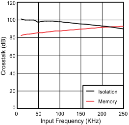
| Channel-to-channel crosstalk | Any off-channel with 100 kHz. Full-scale input to channel being sampled with DC input (isolation crosstalk). | –95 | dB | ||||
| From previously sampled to channel with 100 kHz. Full-scale input to channel being sampled with DC input (memory crosstalk). | –85 | dB | |||||
| EXTERNAL REFERENCE INPUT | |||||||
| Vref | Reference voltage at REFP(5) | 2 | 2.5 | 3 | V | ||
| Rref | Reference resistance | 100 | kΩ | ||||
| ALARM SETTING | |||||||
| Higher threshold range | 0 | FFC | Hex | ||||
| Lower threshold range | 0 | FFC | Hex | ||||
| DIGITAL INPUT/OUTPUT (CMOS Logic Family) | |||||||
| VIH | High logic-level input voltage | 0.7 × V(+VBD) | V | ||||
| VIL | Low logic-level input voltage | V(+VA) = 5 V | 0.8 | V | |||
| V(+VA) = 3 V | 0.4 | V | |||||
| VOH | High logic-level output voltage | At source current (IS) = 200 μA | V(+VBD) – 0.2 | V | |||
| VOL | Low logic-level output voltage | At Isink = 200 μA | 0.4 | V | |||
| Data format MSB first | MSB first | ||||||
| POWER SUPPLY REQUIREMENTS | |||||||
| V(+VA) | Analog power-supply voltage | 2.7 | 3.3 | 5.25 | V | ||
| V(+VBD) | Digital I/O-supply voltage | 1.7 | 3.3 | V(+VA) | V | ||
| I(+VA) | Supply current (normal mode) | At V(+VA) = 2.7 V to 3.6 V and 1-MHz throughput | 1.8 | mA | |||
| At V(+VA) = 2.7 V to 3.6 V static state | 1.05 | mA | |||||
| At V(+VA) = 4.7 V to 5.25 V and 1-MHz throughput | 2.3 | 3 | mA | ||||
| At V(+VA) = 4.7 V to 5.25 V static state | 1.1 | 1.5 | mA | ||||
| Power-down state supply current | 1 | μA | |||||
| I(+VBD) | Digital I/O-supply current | V(+VA) = 5.25 V, ƒsample = 1 MHz | 1 | mA | |||
| Power-up time | 1 | µs | |||||
| Invalid conversions after power up or reset | 1 | cycle | |||||
| Latch-up | JESD78 class I | ||||||
| TEMPERATURE RANGE | |||||||
| Specified performance | –40 | 125 | °C | ||||
(1) Ideal input span; does not include gain or offset error.
(2) LSB means least-significant bit.
(3) Measured relative to an ideal full-scale input
(4) Calculated on the first nine harmonics of the input frequency.
(5) The device is designed to operate over Vref = 2 V to 3 V. However, lower noise performance can be expected at Vref < 2.4 V, because of SNR degradation resulting from lowered signal range.
7.6 Electrical Characteristics: ADS7954-Q1, ADS7956-Q1, ADS7957-Q1
V(+VA) = 2.7 V to 5.25 V, V(+VBD) = 1.7 V to V(+VA), Vref = 2.5 V ± 0.1 V, TA = –40°C to 125°C, ƒsample = 1 MHz (unless otherwise noted)| PARAMETER | TEST CONDITIONS | MIN | TYP | MAX | UNIT | ||
|---|---|---|---|---|---|---|---|
| ANALOG INPUT | |||||||
| Full-scale input span(1) | Range 1 | 0 | Vref | V | |||
| Range 2 while 2 × Vref ≤ +VA | 0 | 2 × Vref | V | ||||
| Absolute input range | Range 1 | –0.2 | Vref + 0.2 | V | |||
| Range 2 while 2 × Vref ≤ +VA | –0.2 | 2 × Vref +0.2 | V | ||||
| Input capacitance | 15 | ρF | |||||
| Input leakage current | TA = 125°C | 61 | nA | ||||
| SYSTEM PERFORMANCE | |||||||
| Resolution | 10 | Bits | |||||
| No missing codes | 10 | Bits | |||||
| Integral linearity | –0.5 | ±0.2 | 0.5 | LSB(2) | |||
| Differential linearity | –0.5 | ±0.2 | 0.5 | LSB | |||
| Offset error(3) | –1.5 | ±0.5 | 1.5 | LSB | |||
| Gain error | Range 1 | –1 | ±0.1 | 1 | LSB | ||
| Range 2 | ±0.1 | LSB | |||||
| SAMPLING DYNAMICS | |||||||
| Conversion time | 20-MHz SCLK | 800 | ns | ||||
| Acquisition time | 325 | ns | |||||
| Maximum throughput rate | 20-MHz SCLK | 1 | MHz | ||||
| Aperture delay | 5 | ns | |||||
| Step response | 150 | ns | |||||
| Over voltage recovery | 150 | ns | |||||
| DYNAMIC CHARACTERISTICS | |||||||
| THD | Total harmonic distortion(4) | 100 kHz | –80 | dB | |||
| SNR | Signal-to-noise ratio | 100 kHz | 60 | dB | |||
| SINAD | Signal-to-noise + distortion | 100 kHz | 60 | dB | |||
| SFDR | Spurious-free dynamic range | 100 kHz | 82 | dB | |||
| Full-power bandwidth | At –3 dB | 47 | MHz | ||||
| Channel-to-channel crosstalk | Any off-channel with 100 kHz. Full-scale input to channel being sampled with dc input. | –95 | dB | ||||
| From previously sampled to channel with 100 kHz. Full-scale input to channel being sampled with dc input. | –85 | dB | |||||
| EXTERNAL REFERENCE INPUT | |||||||
| Vref | Reference voltage at REFP | 2 | 2.5 | 3 | V | ||
| Rref | Reference resistance | 100 | kΩ | ||||
| ALARM SETTING | |||||||
| Higher threshold range | 000 | FFC | Hex | ||||
| Lower threshold range | 000 | FFC | Hex | ||||
| DIGITAL INPUT/OUTPUT (CMOS Logic Family) | |||||||
| VIH | High logic-level input voltage | 0.7 × V(+VBD) | V | ||||
| VIL | Low logic-level input voltage | V(+VBD) = 5 V | 0.8 | V | |||
| V(+VBD) = 3 V | 0.4 | V | |||||
| VOH | High logic-level output voltage | At source current (IS) = 200 μA | V(+VBD) – 0.2 | V | |||
| VOL | Low logic-level output voltage | At Isink = 200 μA | 0.4 | V | |||
| Data format MSB first | MSB first | ||||||
| POWER SUPPLY REQUIREMENTS | |||||||
| V(+VA) | Analog power-supply voltage | 2.7 | 3.3 | 5.25 | V | ||
| V(+VBD) | Digital I/O-supply voltage | 1.7 | 3.3 | V(+VA) | V | ||
| I(+VA) | Supply current (normal mode) | At V(+VA) = 2.7 V to 3.6 V and 1-MHz throughput | 1.8 | mA | |||
| At V(+VA) = 2.7 V to 3.6 V static state | 1.05 | 1 | mA | ||||
| At V(+VA) = 4.7 V to 5.25 V and 1-MHz throughput | 2.3 | 3 | mA | ||||
| At V(+VA) = 4.7 V to 5.25 V static state | 1.1 | 1.5 | mA | ||||
| Power-down state supply current | 1 | μA | |||||
| I(+VBD) | Digital I/O-supply current | V(+VA) = 5.25 V, ƒsample = 1 MHz | 1 | mA | |||
| Power-up time | 1 | μs | |||||
| Invalid conversions after power up or reset | 1 | cycle | |||||
| Latch-up | JESD78 class I | ||||||
| TEMPERATURE RANGE | |||||||
| Specified performance | –40 | 125 | °C | ||||
(1) Ideal input span; does not include gain or offset error.
(2) LSB means least significant bit.
(3) Measured relative to an ideal full-scale input
(4) Calculated on the first nine harmonics of the input frequency.
7.7 Electrical Characteristics: ADS7958-Q1, ADS7959-Q1, ADS7960-Q1, ADS7961-Q1
V(+VA) = 2.7 V to 5.25 V, V(+VBD) = 1.7 V to V(+VA), Vref = 2.5 V ± 0.1 V, TA = –40°C to 125°C, ƒsample = 1 MHz (unless otherwise noted)| PARAMETER | TEST CONDITIONS | MIN | TYP | MAX | UNIT | ||
|---|---|---|---|---|---|---|---|
| ANALOG INPUT | |||||||
| Full-scale input span(1) | Range 1 | 0 | Vref | V | |||
| Range 2 while 2 × Vref ≤ +VA | 0 | 2 × Vref | V | ||||
| Absolute input range | Range 1 | –0.20 | Vref + 0.2 | V | |||
| Range 2 while 2 × Vref ≤ +VA | –0.20 | 2 × Vref + 0.2 | V | ||||
| Input capacitance | 15 | ρF | |||||
| Input leakage current | TA = 125°C | 61 | nA | ||||
| SYSTEM PERFORMANCE | |||||||
| Resolution | 8 | Bits | |||||
| No missing codes | 8 | Bits | |||||
| Integral linearity | –0.3 | ±0.1 | 0.3 | LSB(2) | |||
| Differential linearity | –0.3 | ±0.1 | 0.3 | LSB | |||
| Offset error(3) | –0.5 | ±0.2 | 0.5 | LSB | |||
| Gain error | Range 1 | –0.6 | ±0.1 | 0.6 | LSB | ||
| Range 2 | ±0.1 | LSB | |||||
| SAMPLING DYNAMICS | |||||||
| Conversion time | 20-MHz SCLK | 800 | ns | ||||
| Acquisition time | 325 | ns | |||||
| Maximum throughput rate | 20-MHz SCLK | 1 | MHz | ||||
| Aperture delay | 5 | ns | |||||
| Step response | 150 | ns | |||||
| Over voltage recovery | 150 | ns | |||||
| DYNAMIC CHARACTERISTICS | |||||||
| THD | Total harmonic distortion(4) | 100 kHz | –75 | dB | |||
| SNR | Signal-to-noise ratio | 100 kHz | 49 | dB | |||
| SINAD | Signal-to-noise + distortion | 100 kHz | 49 | dB | |||
| SFDR | Spurious-free dynamic range | 100 kHz | –78 | dB | |||
| Full-power bandwidth | At –3 dB | 47 | MHz | ||||
| Channel-to-channel crosstalk | Any off-channel with 100 kHz. Full-scale input to channel being sampled with dc input. | –95 | dB | ||||
| From previously sampled to channel with 100 kHz. Full-scale input to channel being sampled with dc input. | –85 | dB | |||||
| EXTERNAL REFERENCE INPUT | |||||||
| Vref | reference voltage at REFP | 2 | 2.5 | 3 | V | ||
| Reference resistance | 100 | kΩ | |||||
| ALARM SETTING | |||||||
| Higher threshold range | 000 | FF | Hex | ||||
| Lower threshold range | 000 | FF | Hex | ||||
| DIGITAL INPUT/OUTPUT (CMOS Logic Family) | |||||||
| VIH | High logic-level input voltage | 0.7 × V(+VBD) | V | ||||
| VIL | Low logic-level input voltage | V(+VBD) = 5 V | 0.8 | V | |||
| V(+VBD) = 3 V | 0.4 | V | |||||
| VOH | High logic-level output voltage | At source current (IS) = 200 μA | V(+VBD) – 0.2 | V | |||
| VOL | Low logic-level output voltage | At Isink = 200 μA | 0.4 | V | |||
| Data format | MSB first | ||||||
| POWER SUPPLY REQUIREMENTS | |||||||
| V(+VA) | Analog power-supply voltage | 2.7 | 3.3 | 5.25 | V | ||
| V(+VBD) | Digital I/O-supply voltage | 1.7 | 3.3 | V(+VA) | V | ||
| I(+VA) | Supply current (normal mode) | At V(+VA) = 2.7 V to 3.6 V and 1-MHz throughput | 1.8 | mA | |||
| At V(+VA) = 2.7 V to 3.6 V static state | 1.05 | mA | |||||
| At V(+VA) = 4.7 V to 5.25 V and 1-MHz throughput | 2.3 | 3 | mA | ||||
| At V(+VA) = 4.7 V to 5.25 V static state | 1.1 | 1.5 | mA | ||||
| Power-down state supply current | 1 | μA | |||||
| I(+VBD) | Digital I/O-supply current | V(+VA) = 5.25 V, ƒsample = 1 MHz | 1 | mA | |||
| Power-up time | 1 | μs | |||||
| Invalid conversions after power up or reset | 1 | cycle | |||||
| Latch-up | JESD78 class I | ||||||
| TEMPERATURE RANGE | |||||||
| Specified performance | –40 | 125 | °C | ||||
(1) Ideal input span; does not include gain or offset error.
(2) LSB means least significant bit.
(3) Measured relative to an ideal full-scale input
(4) Calculated on the first nine harmonics of the input frequency.
7.8 Timing Requirements
All specifications typical at –40°C to 125°C, V(+VA) = 2.7 V to 5.25 V (unless otherwise specified). See Figure 45, Figure 46, Figure 47, and Figure 48.| PARAMETER(1)(2) | MIN | TYP | MAX | UNIT | ||
|---|---|---|---|---|---|---|
| tc | Conversion time | V(+VBD) = 1.8 V | 16 | SCLK | ||
| V(+VBD) = 3 V | 16 | SCLK | ||||
| V(+VBD) = 5 V | 16 | SCLK | ||||
| tq | Minimum quiet sampling time needed from bus Tri-state to start of next conversion | V(+VBD) = 1.8 V | 40 | ns | ||
| V(+VBD) = 3 V | 40 | ns | ||||
| V(+VBD) = 5 V | 40 | ns | ||||
| td1 | Delay time, CS low to first data (DO–15) out | V(+VBD) = 1.8 V | 38 | ns | ||
| V(+VBD) = 3 V | 27 | ns | ||||
| V(+VBD) = 5 V | 17 | ns | ||||
| tsu1 | Setup time, CS low to first rising edge of SCLK | V(+VBD) = 1.8 V | 8 | ns | ||
| V(+VBD) = 3 V | 6 | ns | ||||
| V(+VBD) = 5 V | 4 | ns | ||||
| td2 | Delay time, SCLK falling to SDO next data bit valid | V(+VBD) = 1.8 V | 35 | ns | ||
| V(+VBD) = 3 V | 27 | ns | ||||
| V(+VBD) = 5 V | 17 | ns | ||||
| th1 | Hold time, SCLK falling to SDO data bit valid | V(+VBD) = 1.8 V | 7 | ns | ||
| V(+VBD) = 3 V | 5 | ns | ||||
| V(+VBD) = 5 V | 3 | ns | ||||
| td3 | Delay time, 16th SCLK falling edge to SDO 3-state | V(+VBD) = 1.8 V | 26 | ns | ||
| V(+VBD) = 3 V | 22 | ns | ||||
| V(+VBD) = 5 V | 13 | ns | ||||
| tsu2 | Setup time, SDI valid to rising edge of SCLK | V(+VBD) = 1.8 V | 2 | ns | ||
| V(+VBD) = 3 V | 3 | ns | ||||
| V(+VBD) = 5 V | 4 | ns | ||||
| th2 | Hold time, rising edge of SCLK to SDI valid | V(+VBD) = 1.8 V | 12 | ns | ||
| V(+VBD) = 3 V | 10 | ns | ||||
| V(+VBD) = 5 V | 6 | ns | ||||
| tw1 | Pulse duration CS high | V(+VBD) = 1.8 V | 20 | ns | ||
| V(+VBD) = 3 V | 20 | ns | ||||
| V(+VBD) = 5 V | 20 | ns | ||||
| td4 | Delay time CS high to SDO 3-state | V(+VBD) = 1.8 V | 24 | ns | ||
| V(+VBD) = 3 V | 21 | ns | ||||
| V(+VBD) = 5 V | 12 | ns | ||||
| twH | Pulse duration SCLK high | V(+VBD) = 1.8 V | 20 | ns | ||
| V(+VBD) = 3 V | 20 | ns | ||||
| V(+VBD) = 5 V | 20 | ns | ||||
| twL | Pulse duration SCLK low | V(+VBD) = 1.8 V | 20 | ns | ||
| V(+VBD) = 3 V | 20 | ns | ||||
| V(+VBD) = 5 V | 20 | ns | ||||
| ƒ(SCLK) | Frequency SCLK | V(+VBD) = 1.8 V | 20 | MHz | ||
| V(+VBD) = 3 V | 20 | MHz | ||||
| V(+VBD) = 5 V | 20 | MHz | ||||
(1) 1.8-V specifications apply from 1.7 V to 1.9 V, 3-V specifications apply from 2.7 V to 3.6 V, 5-V specifications apply from 4.75 V to 5.25 V.
(2) With 50-pF load
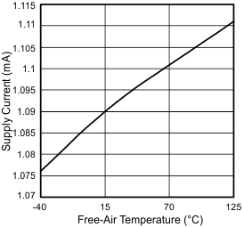
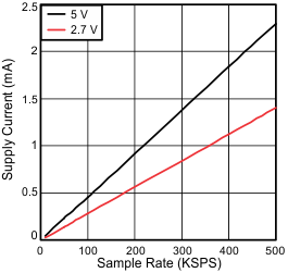
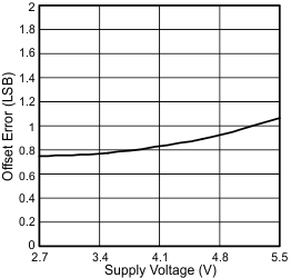
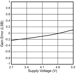
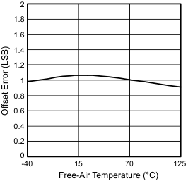
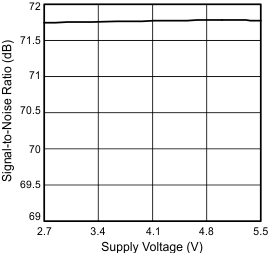
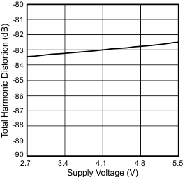
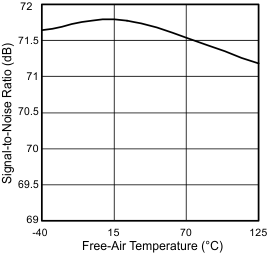
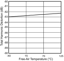
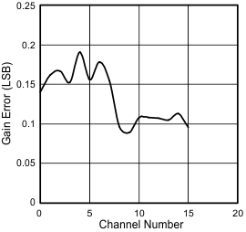
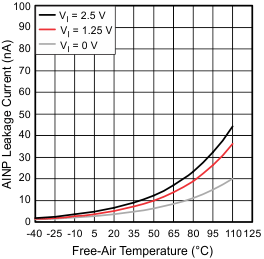
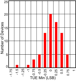
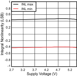
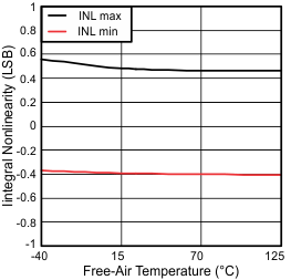
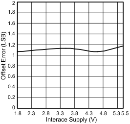
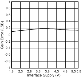
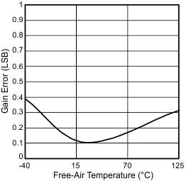
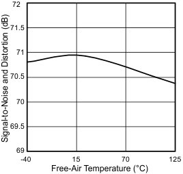
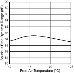
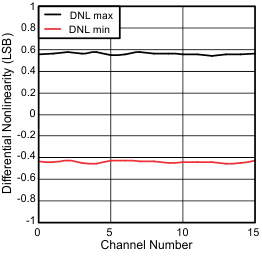
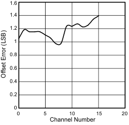
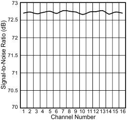
7.9 Typical Characteristics (All ADS79xx-Q1 Family Devices)
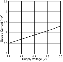
| ƒsample = 1 MSPS | TA = 25°C |
| ƒsample = 1 MSPS | V(+VBD) = 5.5 V |
| No power-down | TA = 25°C | |
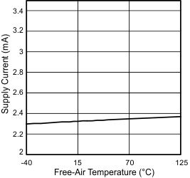
| ƒsample = 0 MSPS | TA = 25°C |
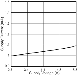
| ƒsample = 0 MSPS | V(+VBD) = 5.5 V |
Free-Air Temperature
| With power-down mode enabled | TA = 25°C | |
Power-Down Mode Enabled
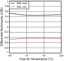
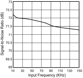
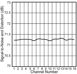
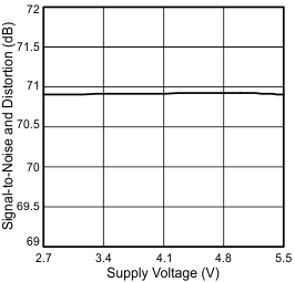
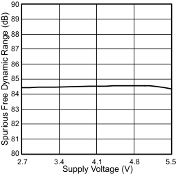
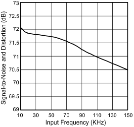
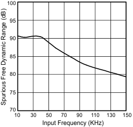
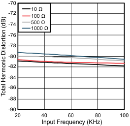
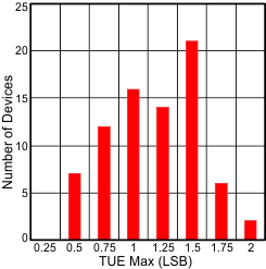
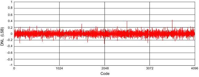
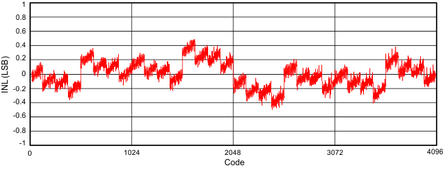
7.10 Typical Characteristics (12-Bit Devices Only)
Variations for 10-bit and 8-bit devices are too small to be illustrated through the characteristic curves.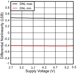
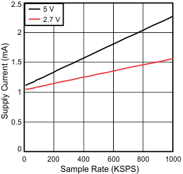
| ƒsample = 1 MSPS | TA = 25°C |
| ƒsample = 1 MSPS | V(+VA) = 5 V | V(+VBD) = 5 V |
| ƒsample = 1 MSPS | TA = 25°C | V(+VBD) = 1.8 V |
| ƒsample = 1 MSPS | TA = 25°C | V(+VBD) = 1.8 V |
| ƒsample = 1 MSPS | V(+VA) = 5.5 V | V(+VBD) = 1.8 V |
| ƒsample = 1 MSPS | TA = 25°C | V(+VBD) = 3 V |
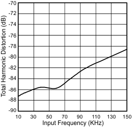
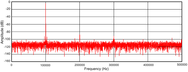
| ƒinput = 100 kHz |
| ƒsample = 1 MSPS | TA = 25°C | V(+VBD) = 3 V |
| ƒinput = 100 kHz |
| ƒsample = 1 MSPS | V(+VA) = 5 V | V(+VBD) = 3 V |
| ƒinput = 100 kHz |
| ƒsample = 1 MSPS | V(+VA) = 5 V | V(+VBD) = 3 V |
| ƒinput = 100 kHz |
| ƒsample = 1 MSPS | V(+VA) = 5 V | V(+VBD) = 3 V |
| TA = 25°C | MXO shorted to AINP | |
| ƒsample = 1 MSPS | V(+VA) = 5 V | V(+VBD) = 3 V |
| TA = 25°C | MXO shorted to AINP | |
| ƒsample = 1 MSPS | V(+VA) = 5 V | V(+VBD) = 5 V |
| TA = 25°C | Buffer between MXO and AINP | |
| ƒsample = 1 MSPS | V(+VA) = 5 V | V(+VBD) = 5 V |
| TA = 25°C | Buffer between MXO and AINP | |
| ƒsample = 1 MSPS | V(+VA) = 5 V | V(+VBD) = 5 V |
| ƒsample = 1 MSPS | V(+VA) = 5 V | V(+VBD) = 5 V |
| ƒsample = 1 MSPS | V(+VA) = 5 V | V(+VBD) = 5 V |
| V(+VA) = 5 V | V(+VBD) = 5 V |
| ƒsample = 1 MSPS | TA = 25°C |
| ƒsample = 1 MSPS | V(+VA) = 5 V | V(+VBD) = 5 V |
| ƒsample = 1 MSPS | TA = 25°C | V(+VA) = 5.5 V |
| ƒsample = 1 MSPS | TA = 25°C | V(+VA) = 5.5 V |
| ƒsample = 1 MSPS | V(+VA) = 5.5 V | V(+VBD) = 1.8 V |
| ƒsample = 1 MSPS | TA = 25°C | V(+VBD) = 3 V |
| ƒinput = 100 kHz |
| ƒsample = 1 MSPS | TA = 25°C | V(+VBD) = 3 V |
| ƒinput = 100 kHz |
| ƒsample = 1 MSPS | V(+VA) = 5 V | V(+VBD) = 3 V |
| ƒinput = 100 kHz |
| ƒsample = 1 MSPS | V(+VA) = 5 V | V(+VBD) = 3 V |
| ƒinput = 100 kHz |
| ƒsample = 1 MSPS | V(+VA) = 5 V | V(+VBD) = 3 V |
| TA = 25°C | MXO shorted to AINP | |
| ƒsample = 1 MSPS | V(+VA) = 5 V | V(+VBD) = 3 V |
| TA = 25°C | MXO shorted to AINP | |
| ƒsample= 1 MSPS | V(+VA) = 5 V | V(+VBD) = 5 V |
| TA = 25°C | Buffer between MXO and AINP | |
| ƒsample = 1 MSPS | V(+VA) = 5 V | V(+VBD) = 5 V |
| ƒsample = 1 MSPS | V(+VA) = 5 V | V(+VBD) = 5 V |
| ƒsample = 1 MSPS | V(+VA) = 5 V | V(+VBD) = 5 V |
| ƒsample = 1 MSPS | V(+VA) = 5 V | V(+VBD) = 5 V |
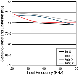
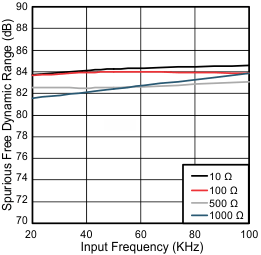
| CH0, CH1 |
| ƒsample = 1 MSPS | V(+VA) = 5 V | V(+VBD) = 5 V | ||
| TA = 25°C | ||||
| ƒsample = 1 MSPS | V(+VA) = 5 V | V(+VBD) = 5 V | ||
| ƒsample = 1 MSPS | V(+VA) = 5 V | V(+VBD) = 5 V | ||
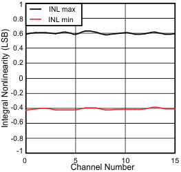
| ƒinput = 100 kHz | Npoints = 16,384 | |||