JAJSHL6E August 2010 – June 2019 AFE031
PRODUCTION DATA.
- 1 特長
- 2 アプリケーション
- 3 概要
- 4 改訂履歴
- 5 概要 (続き)
- 6 Device Comparison Table
- 7 Pin Configuration and Functions
-
8 Specifications
- 8.1 Absolute Maximum Ratings
- 8.2 ESD Ratings
- 8.3 Thermal Information
- 8.4 Electrical Characteristics: Transmitter (Tx)
- 8.5 Electrical Characteristics: Power Amplifier (PA)
- 8.6 Electrical Characteristics: Receiver (Rx)
- 8.7 Electrical Characteristics: Digital
- 8.8 Electrical Characteristics: Two-Wire Interface
- 8.9 Electrical Characteristics: Internal Bias Generator
- 8.10 Electrical Characteristics: Power Supply
- 8.11 Timing Requirements
- 8.12 Timing Diagrams
- 8.13 Typical Characteristics
- 9 Detailed Description
- 10Application and Implementation
- 11デバイスおよびドキュメントのサポート
- 12メカニカル、パッケージ、および注文情報
パッケージ・オプション
メカニカル・データ(パッケージ|ピン)
- RGZ|48
サーマルパッド・メカニカル・データ
- RGZ|48
発注情報
9.2.7 ETx and ERx Blocks
The AFE031 contains a two-wire transmitter block, ETx, and a two-wire receiver block, ERx. These blocks support communications that use amplitude shift keying (ASK) with on-off keying (OOK) modulation.
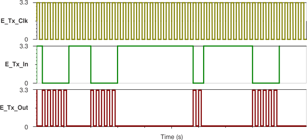
The ETx block is a gated driver that allows for transmission of a carrier input signal and modulating input signal. For typical applications, a 50-kHz square wave carrier signal is applied to E_Tx_Clk while the modulating signal is applied to E_Tx_In. The output (E_Tx_Out) is then in a high-impedance state when E_Tx_In is '1'. Figure 41 shows the relationship between E_Tx_Clk, E_Tx_In, and E_Tx_Out.
 Figure 41. ETx Block Transfer Function
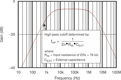
 The ERx Block consists of a low-pass analog filter configured in an inverting gain of –4.5 db. This block, along with an external capacitor, can be used to create a passband filter response as shown in Figure 42.
 Figure 42. ERx Block Frequency Response
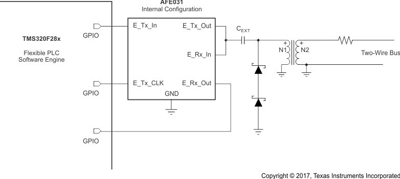
 The E_Rx_Out pin can be directly connected to either an available analog-to-digital converter (ADC) input or GPIO on the host microcontroller. Figure 43 illustrates a typical two-wire application for ETx and ERx.
 Figure 43. Typical Two-Wire Application for ETx and ERx