JAJSE30A October 2017 – June 2018 AMC1106E05 , AMC1106M05
PRODUCTION DATA.
- 1 特長
- 2 アプリケーション
- 3 概要
- 4 改訂履歴
- 5 Device Comparison Table
- 6 Pin Configuration and Functions
-
7 Specifications
- 7.1 Absolute Maximum Ratings
- 7.2 ESD Ratings
- 7.3 Recommended Operating Conditions
- 7.4 Thermal Information
- 7.5 Power Ratings
- 7.6 Insulation Specifications
- 7.7 Safety-Related Certifications
- 7.8 Safety Limiting Values
- 7.9 Electrical Characteristics: AMC1106x
- 7.10 Timing Requirements
- 7.11 Switching Characteristics
- 7.12 Insulation Characteristics Curves
- 7.13 Typical Characteristics
- 8 Detailed Description
- 9 Application and Implementation
- 10Power Supply Recommendations
- 11Layout
- 12デバイスおよびドキュメントのサポート
- 13メカニカル、パッケージ、および注文情報
8.3.3 Isolation Channel Signal Transmission
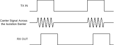
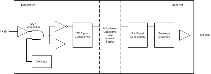
The AMC1106 uses an on-off keying (OOK) modulation scheme to transmit the modulator output bitstream across the capacitive SiO2-based isolation barrier. The transmitter modulates the bitstream at TX IN in Figure 43 with an internally-generated, 480-MHz carrier across the isolation barrier to represent a digital one and sends a no signal to represent the digital zero. The receiver demodulates the signal after advanced signal conditioning and produces the output. The symmetrical design of each isolation channel improves the CMTI performance and reduces the radiated emissions caused by the high-frequency carrier. Figure 43 shows a block diagram of an isolation channel integrated in the AMC1106.
Figure 44 shows the concept of the on-off keying scheme.
 Figure 44. OOK-Based Modulation Scheme