SBASA51 May 2020 AMC1336-Q1
PRODUCTION DATA.
- 1 Features
- 2 Applications
- 3 Description
- 4 Revision History
- 5 Pin Configuration and Functions
-
6 Specifications
- Table 1. Absolute Maximum Ratings
- Table 2. ESD Ratings
- Table 3. Recommended Operating Conditions
- Table 4. Thermal Information
- Table 5. Power Ratings
- Table 6. Insulation Specifications
- Table 7. Safety-Related Certifications
- Table 8. Safety Limiting Values
- Table 9. Electrical Characteristics
- Table 10. Switching Characteristics
- 6.1 Insulation Characteristics Curves
- 6.2 Typical Characteristics
- 7 Detailed Description
- 8 Application and Implementation
- 9 Power Supply Recommendations
- 10Layout
- 11Device and Documentation Support
- 12Mechanical, Packaging, and Orderable Information
8.2 Typical Application
Isolated ΔΣ modulators are widely used in onboard charger (OBC) and traction inverter designs because of their high AC and DC performance. The input structure of the AMC1336-Q1 is optimized for use with high-impedance resistor dividers. The ±1-V, differential input enables sensing of positive and negative voltages in the system.
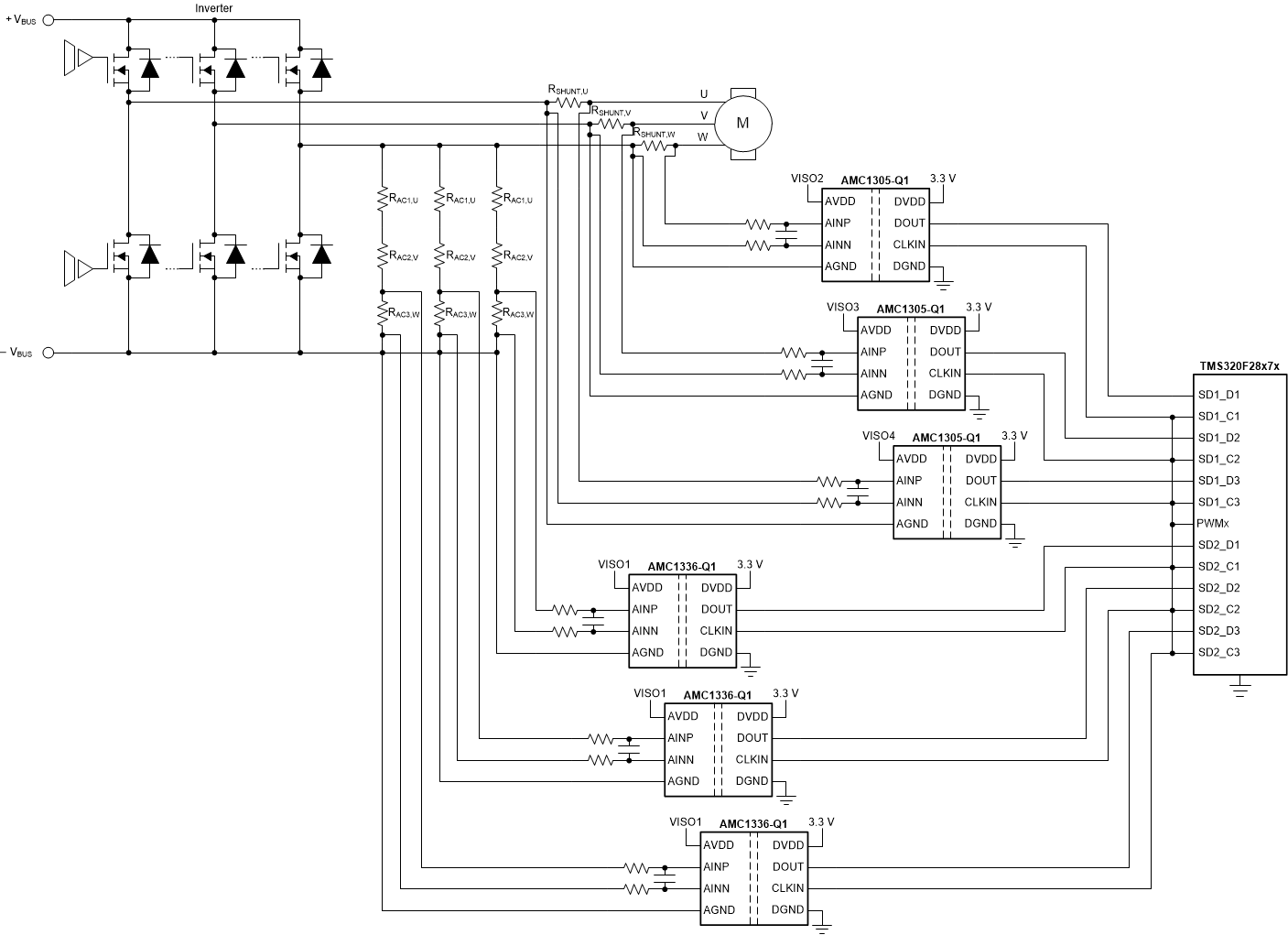
Figure 50 shows a simplified schematic of a traction inverter application with the AMC1336-Q1 used for output phase voltage sensing. In this example, the ground reference point for the microcontroller is not connected by any means to the power stage. This configuration is usually the case in systems with the microcontroller located on a dedicated control card or PCB.
Current feedback is performed with shunt resistors (RSHUNT) and TI's AMC1305M05-Q1 isolated modulators. Depending on the system design, either all three or only two motor phase currents are sensed.
Depending on the overall digital processing power requirements and with a total of eight ΔΣ modulator bitstreams to be processed by the microcontroller (MCU), a derivate from either the low-cost single-core TMS320F2807x or the dual-core TMS320F2837x families can be used in this application.
 Figure 50. The AMC1336-Q1 in a Frequency Inverter Application
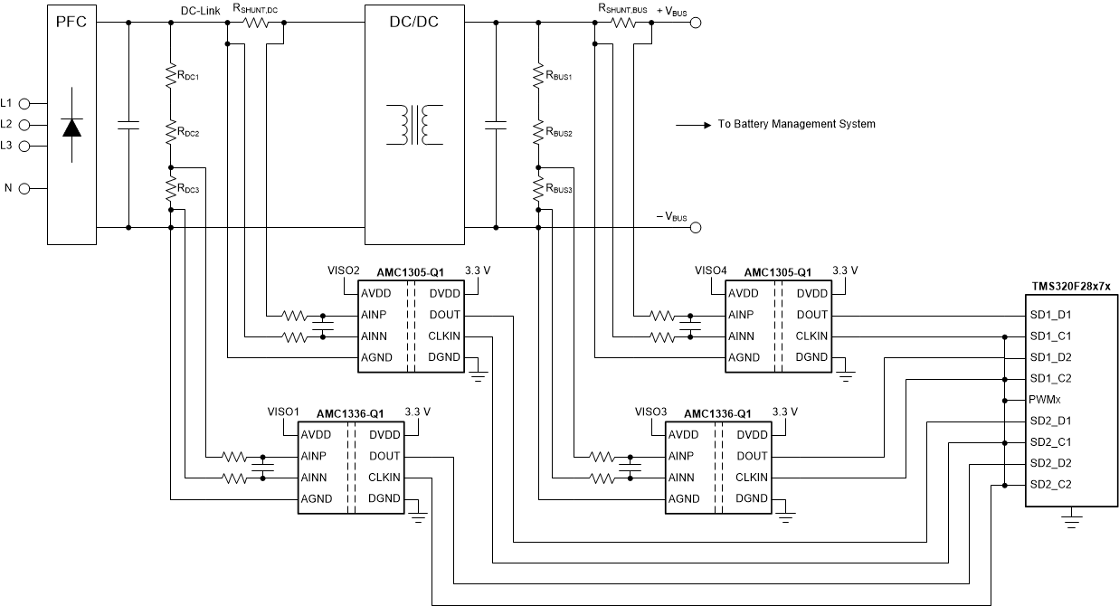
 Figure 51 shows an additional example of the AMC1336-Q1 used for DC-link and VBUS voltage sensing in an onboard charger. Also in this case, the microcontroller is located on a dedicated control card and the AMC1305M05-Q1 is used for shunt-based current sensing.
 Figure 51. The in an On-Board Charger Application