JAJSJE2A july   2020  – april 2023 BQ21062

PRODUCTION DATA  

  1.   1
  2. 特長
  3. アプリケーション
  4. 概要
  5. Revision History
  6. 概要 (続き)
  7. Device Comparison Table
  8. Pin Configuration and Functions
  9. Specifications
    1. 8.1 Absolute Maximum Ratings
    2. 8.2 ESD Ratings
    3. 8.3 Recommended Operating Conditions
    4. 8.4 Thermal Information
    5. 8.5 Electrical Characteristics
    6. 8.6 Timing Requirements
    7. 8.7 Typical Characteristics
  10. Detailed Description
    1. 9.1 Overview
    2. 9.2 Functional Block Diagram
    3. 9.3 Feature Description
      1. 9.3.1  Linear Charger and Power Path
        1. 9.3.1.1 Battery Charging Process
        2. 9.3.1.2 JEITA and Battery Temperature Dependent Charging
        3. 9.3.1.3 Input Voltage Based Dynamic Power Management (VINDPM)
        4. 9.3.1.4 Battery Supplement Mode
      2. 9.3.2  Protection Mechanisms
        1. 9.3.2.1 Input Over-Voltage Protection
        2. 9.3.2.2 Safety Timer and I2C Watchdog Timer
        3. 9.3.2.3 Thermal Protection and Thermal Charge Current Foldback
        4. 9.3.2.4 Battery Short and Over Current Protection
        5. 9.3.2.5 PMID Short Circuit
      3. 9.3.3  VDD LDO
      4. 9.3.4  Load Switch/LDO Output and Control
      5. 9.3.5  PMID Power Control
      6. 9.3.6  System Voltage (PMID) Regulation
      7. 9.3.7  MR Wake and Reset Input
        1. 9.3.7.1 MR Wake or Short Button Press Functions
        2. 9.3.7.2 MR Reset or Long Button Press Functions
      8. 9.3.8  14-Second Watchdog for HW Reset
      9. 9.3.9  Faults Conditions and Interrupts ( INT)
        1. 9.3.9.1 Flags and Fault Condition Response
      10. 9.3.10 Power Good ( PG) Pin
      11. 9.3.11 External NTC Monitoring (TS)
        1. 9.3.11.1 TS Thresholds
      12. 9.3.12 I2C Interface
        1. 9.3.12.1 F/S Mode Protocol
    4. 9.4 Device Functional Modes
      1. 9.4.1 Ship Mode
      2. 9.4.2 Low Power
      3. 9.4.3 Active Battery
      4. 9.4.4 Charger/Adapter Mode
      5. 9.4.5 Power-Up/Down Sequencing
    5. 9.5 Register Map
      1. 9.5.1 I2C Registers
  11. 10Application and Implementation
    1. 10.1 Application Information
    2. 10.2 Typical Application
      1. 10.2.1 Design Requirements
      2. 10.2.2 Detailed Design Procedure
        1. 10.2.2.1 Input (IN/PMID) Capacitors
        2. 10.2.2.2 VDD, LDO Input and Output Capacitors
        3. 10.2.2.3 TS
        4. 10.2.2.4 Recommended Passive Components
      3. 10.2.3 Application Curves
  12. 11Power Supply Recommendations
  13. 12Layout
    1. 12.1 Layout Guidelines
    2. 12.2 Layout Example
  14. 13Device and Documentation Support
    1. 13.1 Device Support
      1. 13.1.1 サード・パーティ製品に関する免責事項
    2. 13.2 Documentation Support
      1. 13.2.1 Related Documentation
    3. 13.3 ドキュメントの更新通知を受け取る方法
    4. 13.4 サポート・リソース
    5. 13.5 Trademarks
    6. 13.6 静電気放電に関する注意事項
    7. 13.7 用語集
  15. 14Mechanical, Packaging, and Orderable Information

デバイスごとのパッケージ図は、PDF版データシートをご参照ください。

メカニカル・データ(パッケージ|ピン)
  • YFP|20
サーマルパッド・メカニカル・データ

Power-Up/Down Sequencing

The power-up and power-down sequences for the BQ21062 are shown below. Upon VIN insertion, VIN> VUVLO, the device wakes up, powering the VDD rail. If VIN > VBAT + VSLP and VIN < VOVP, PMID will be powered by VIN and if VIN > VIN_DPM charging will start if enabled.

In the case where VIN < VUVLO and the battery is inserted (VBAT > VBATUVLO), the device will immediately enter Ship Mode unless MR is held low. Upon battery insertion the VDD rail will come up to allow the device to check the MR state and if MR is high VDD will immediately be disabled and the device will enter Ship Mode. If MR is low, the device will start the WAKE timer and power up PMID and other rails if MR is held low for longer than tWAKE1.
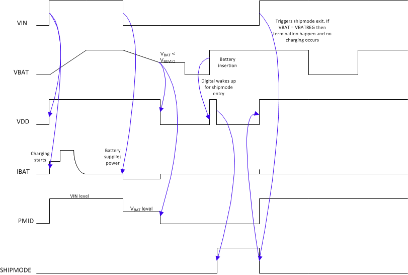
GUID-1BC6E7DE-4461-491D-B440-CAE1BEF81AC2-low.gifFigure 9-14 BQ21062 Wake-Up Upon Supply Insertion
GUID-20220930-SS0I-QL08-BTWB-KLMJNN6901WD-low.svgFigure 9-15 BQ21062 Wake-Up Upon Battery Insertion