SLUS977B September 2009 – August 2015
PRODUCTION DATA.
- 1 Features
- 2 Applications
- 3 Description
- 4 Revision History
- 5 Device Comparison Table
- 6 Pin Configuration and Functions
- 7 Specifications
- 8 Detailed Description
- 9 Application and Implementation
- 10Power Supply Recommendations
- 11Layout
- 12Device and Documentation Support
- 13Mechanical, Packaging, and Orderable Information
パッケージ・オプション
メカニカル・データ(パッケージ|ピン)
- DSG|8
サーマルパッド・メカニカル・データ
- DSG|8
発注情報
9 Application and Implementation
NOTE
Information in the following applications sections is not part of the TI component specification, and TI does not warrant its accuracy or completeness. TI’s customers are responsible for determining suitability of components for their purposes. Customers should validate and test their design implementation to confirm system functionality.
9.1 Application Information
The bq24308 device protects against overvoltage, overcurrent, and battery overvoltage events that occur due to faulty adapter or other input sources. If any of these faults occur, the bq24308 device isolates the downstream devices from the input source.
9.2 Typical Application
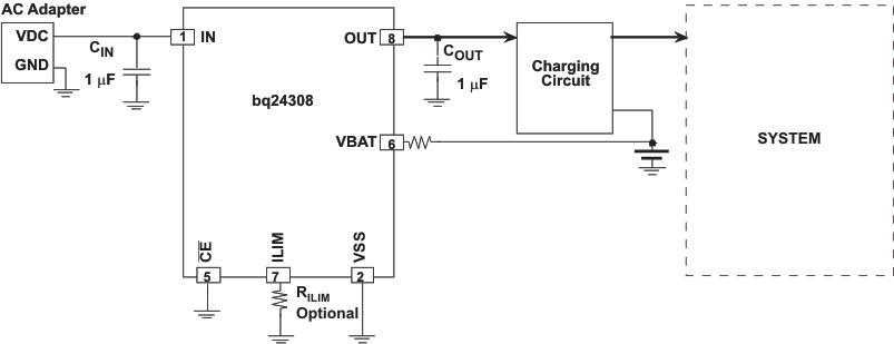
The typical values for an application are VOVP = 6.3 V, IOCP = 700 mA, and BVOVP = 4.35 V.
9.2.1 Design Requirements
For this design example, use the parameters listed in Table 1.
Table 1. Design Parameters
| DESIGN PARAMETER | EXAMPLE VALUE |
|---|---|
| Supply Voltage | 5 V |
| INILIM | 1 A |
9.2.2 Detailed Design Procedure
9.2.2.1 Selection of RBAT
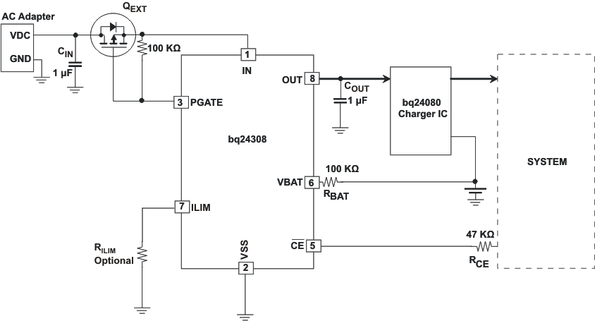
It is strongly recommended that the battery not be tied directly to the VBAT pin of the device, as under some failure modes of the device, the voltage at the IN pin may appear on the VBAT pin. This voltage can be as high as 30 V, and applying 30 V to the battery in case of the failure of the device and can be hazardous. Connecting the VBAT pin through RBAT prevents a large current from flowing into the battery in case of failure of the device. In the interests of safety, RBAT should have a very high value. The problem with a large RBAT is that the voltage drop across this resistor because of the VBAT bias current IVBAT causes an error in the BVOVP threshold. This error is over and above the tolerance on the nominal 4.35-V BVOVP threshold.
Choosing RBAT in the range from 100 KΩ to 470 kΩ is a good compromise. In the case of a device failure, with RBAT equal to 100 kΩ, the maximum current flowing into the battery would be (30 V – 3 V) ÷ 100 kΩ = 270 μA, which is low enough to be absorbed by the bias currents of the system components. RBAT equal to 100 kΩ would result in a worst-case voltage drop of RBAT × IVBAT = 1 mV. This is negligible compared to the internal tolerance of 50 mV on the BVOVP threshold.
If the Bat-OVP function is not required, the VBAT pin should be connected to VSS.
9.2.2.2 Selection of RCE
The CE pin can be used to enable and disable the device. If host control is not required, the CE pin can be tied to ground or left unconnected, permanently enabling the device.
In applications where external control is required, the CE pin can be controlled by a host processor. As in the case of the VBAT pin (see previous discussion), the CE pin should be connected to the host GPIO pin through as large a resistor as possible. The limitation on the resistor value is that the minimum VOH of the host GPIO pin less the drop across the resistor should be greater than VIH of the bq24308 device's CE pin. The drop across the resistor is given by RCE × IIH.
9.2.2.3 Selection of Input and Output Bypass Capacitors
The input capacitor CIN in Figure 12 and Figure 13 is for decoupling and serves an important purpose. Whenever there is a step change downwards in the system load current, the inductance of the input cable causes the input voltage to spike up. CIN prevents the input voltage from overshooting to dangerous levels. It is strongly recommended that a ceramic capacitor of at least 1 μF be used at the input of the device. It should be located in close proximity to the IN pin.
COUT in Figure 12 and Figure 13 is also important: If a very fast (< 1 µs rise-time) overvoltage transient occurs at the input, the current that charges COUT causes the device’s current-limiting loop to kick in, reducing the gate-drive to FET Q1. This results in improved performance for input overvoltage protection. COUT should also be a ceramic capacitor of at least 1 µF, located close to the OUT pin. COUT also serves as the input decoupling capacitor for the charging circuit downstream of the protection device.
 Figure 12. Overvoltage, Overcurrent, and Battery Overvoltage Protection
9.2.2.4 Selection of the PGATE External MOSFET
The PGATE output drives the gate of an external MOSFET to protect the device from reverse polarity input voltages. The MOSFET must be sized to handle the expected current in the application. Additionally, the impedance of the MOSFET is in series with the internal FET of the bq24308, so that the overall acceptable system resistance must be taken into account. Ensure the MOSFET VDS maximum rating exceeds the worst-case expected reverse voltage in the application. The bq24308 withstands up to –30 V, so a 30 V rating on the MOSFET is a good target. The maximum VGS of the MOSFET must be greater than –17 V to ensure operation up to 30 V inputs.
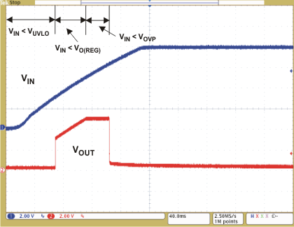
9.2.3 Application Curves
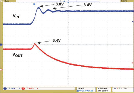
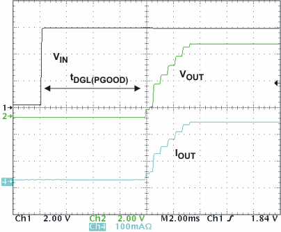
| VIN = 5 V to 8 V | tR = 3 μs |
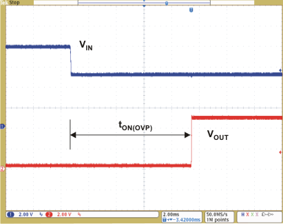
| VIN = 8 V to 5 V | tF = 100 μs |
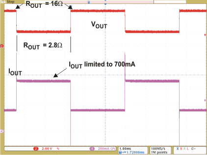
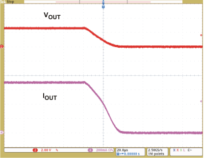
| ROUT Switches from 16 Ω to 2.8 Ω | ||
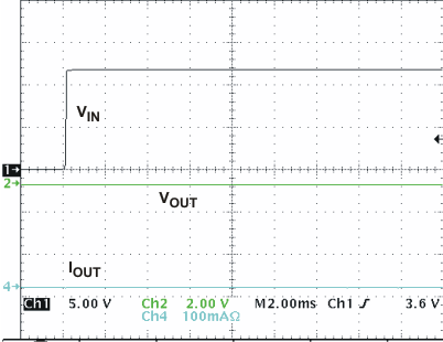
| VIN = 0 V to 12 V | tR = 50 μs | |
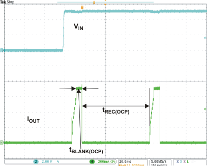
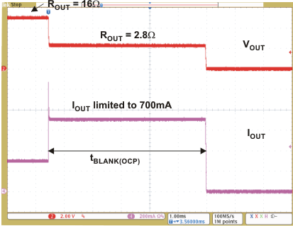
| ROUT Switches from 16 Ω to 2.8 Ω | ||
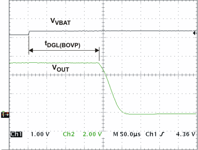
| VVBAT Steps from 4.3 V to 4.5 V. | ||
