SLUSBV8C August 2014 – November 2014
UNLESS OTHERWISE NOTED, this document contains PRODUCTION DATA.
- 1 Features
- 2 Applications
- 3 Description
- 4 Revision History
- 5 Device Comparison Table
- 6 Pin Configuration and Functions
- 7 Specifications
-
8 Detailed Description
- 8.1 Overview
- 8.2 Functional Block Diagram
- 8.3
Feature Description
- 8.3.1 Overvoltage-Protection (OVP) - Continuously Monitored
- 8.3.2 CHG Pin Indication (bq25101, bq25101H)
- 8.3.3 CHG Pin LED Pull-up Source (bq25101, bq25101H)
- 8.3.4 IN-DPM (VIN-DPM or IN-DPM)
- 8.3.5 OUT
- 8.3.6 ISET
- 8.3.7 PRE_TERM - Pre-Charge and Termination Programmable Threshold
- 8.3.8 TS
- 8.3.9 Timers
- 8.3.10 Termination
- 8.4 Device Functional Modes
- 9 Application and Implementation
- 10Power Supply Recommendations
- 11Layout
- 12Device and Documentation Support
- 13Mechanical, Packaging, and Orderable Information
6 Pin Configuration and Functions
6-Pin DSBGA
YFP Package
(Top View)
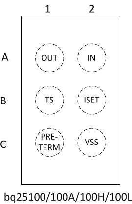 bq25100/bq25100A/bq25100H/bq25100L
6-Pin DSBGA
YFP Package
(Top View)
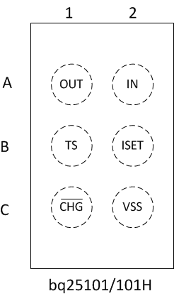 bq25101/bq25101H
Pin Functions
| PIN | I/O | DESCRIPTION | |
|---|---|---|---|
| NAME | NUMBER | ||
| CHG | C1(1) | Low (FET on) indicates charging and open drain (FET off) indicates no charging or the first charge cycle complete. | |
| IN | A2 | I | Input power, connected to external DC supply (AC adapter or USB port). Expected range of bypass capacitors 1 μF to 10 μF, connect from IN to VSS. |
| ISET | B2 | I | Programs the fast-charge current setting. External resistor from ISET to VSS defines fast charge current value. Recommended range is 13.5 kΩ (10 mA) to 0.54 kΩ (250 mA). |
| OUT | A1 | O | Battery Connection. System Load may be connected. Expected range of bypass capacitors 1 μF to 10 μF. |
| PRE-TERM | C1(1) | I | Programs the current termination threshold ( 1% to 50% of Iout, 1mA minimum). The pre-charge current is twice the termination current level. |
| Expected range of programming resistor is 600 Ω to 30 kΩ (6k: Ichg/10 for term; Ichg/5 for precharge) | |||
| TS | B1 | I | Temperature sense pin connected to 10k at 25°C NTC thermistor, in the battery pack. Floating TS pin or pulling high puts part in TTDM “Charger” mode and disables TS monitoring, Timers and Termination. Pulling pin low disables the IC. If NTC sensing is not needed, connect this pin to VSS through an external 10-kΩ resistor. A 250-kΩ resistor from TS to ground will prevent IC entering TTDM mode when battery with thermistor is removed. |
| VSS | C2 | – | Ground pin |
(1) Spins have different pin definitions