JAJSLQ0 November   2021 BQ25173

PRODUCTION DATA  

  1. 特長
  2. アプリケーション
  3. 概要
  4. Revision History
  5. Pin Configuration and Functions
  6. Specifications
    1. 6.1 Absolute Maximum Ratings
    2. 6.2 ESD Ratings
    3. 6.3 Recommended Operating Conditions
    4. 6.4 Thermal Information
    5. 6.5 Electrical Characteristics
    6. 6.6 Timing Requirements
    7. 6.7 Typical Characteristics
  7. Detailed Description
    1. 7.1 Overview
    2. 7.2 Functional Block Diagram
    3. 7.3 Feature Description
      1. 7.3.1 Device Power Up from Input Source
        1. 7.3.1.1 ISET Pin Detection
      2. 7.3.2 Supercapacitor Regulation Voltage
      3. 7.3.3 Supercapacitor Charging Profile
      4. 7.3.4 Status Outputs (PG, STAT)
        1. 7.3.4.1 Power Good Indicator (PG Pin)
        2. 7.3.4.2 Charging Status Indicator (STAT)
      5. 7.3.5 Protection Features
        1. 7.3.5.1 Input Overvoltage Protection (VIN OVP)
        2. 7.3.5.2 Output Overcurrent Protection (OUT OCP)
        3. 7.3.5.3 Thermal Regulation and Thermal Shutdown (TREG and TSHUT)
    4. 7.4 Device Functional Modes
      1. 7.4.1 Shutdown or Undervoltage Lockout (UVLO)
      2. 7.4.2 Sleep Mode
      3. 7.4.3 Active Mode
        1. 7.4.3.1 Standby Mode
      4. 7.4.4 Fault Mode
  8. Application and Implementation
    1. 8.1 Application Information
    2. 8.2 Typical Applications
      1. 8.2.1 1s Supercapacitor Charger Design Example
        1. 8.2.1.1 Design Requirements
        2. 8.2.1.2 Detailed Design Procedure
        3. 8.2.1.3 Application Curves
      2. 8.2.2 4s Supercapacitor Charger Design Example
        1. 8.2.2.1 Design Requirements
        2. 8.2.2.2 Application Curves
  9. Power Supply Recommendations
  10. 10Layout
    1. 10.1 Layout Guidelines
    2. 10.2 Layout Example
    3. 10.3 Thermal Package
  11. 11Device and Documentation Support
    1. 11.1 Device Support
      1. 11.1.1 Third-Party Products Disclaimer
    2. 11.2 Receiving Notification of Documentation Updates
    3. 11.3 サポート・リソース
    4. 11.4 Trademarks
    5. 11.5 Electrostatic Discharge Caution
    6. 11.6 Glossary
  12. 12Mechanical, Packaging, and Orderable Information

パッケージ・オプション

メカニカル・データ(パッケージ|ピン)
サーマルパッド・メカニカル・データ
発注情報

Typical Characteristics

CIN = 1 µF, COUT = 1 µF
GUID-20200827-CA0I-JVLW-ZPSM-CMJKDWSGNTSF-low.gif
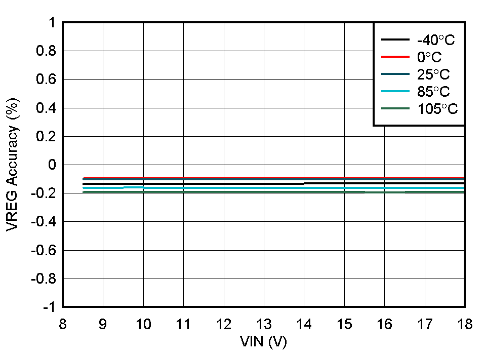
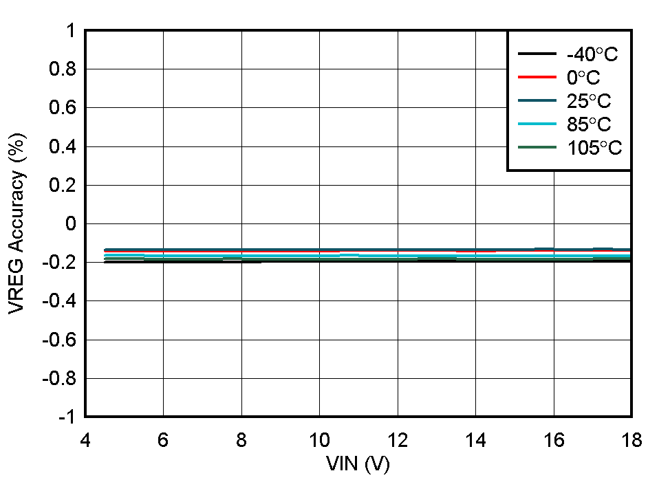
IOUT = 10 mAVOUT = 4.2 V
Figure 6-1 Line Regulation
VIN = 5 VVOUT = 4.2 V
Figure 6-3 Load Regulation
GUID-20210326-CA0I-GN3X-L4CD-QQW5BSZV707R-low.png
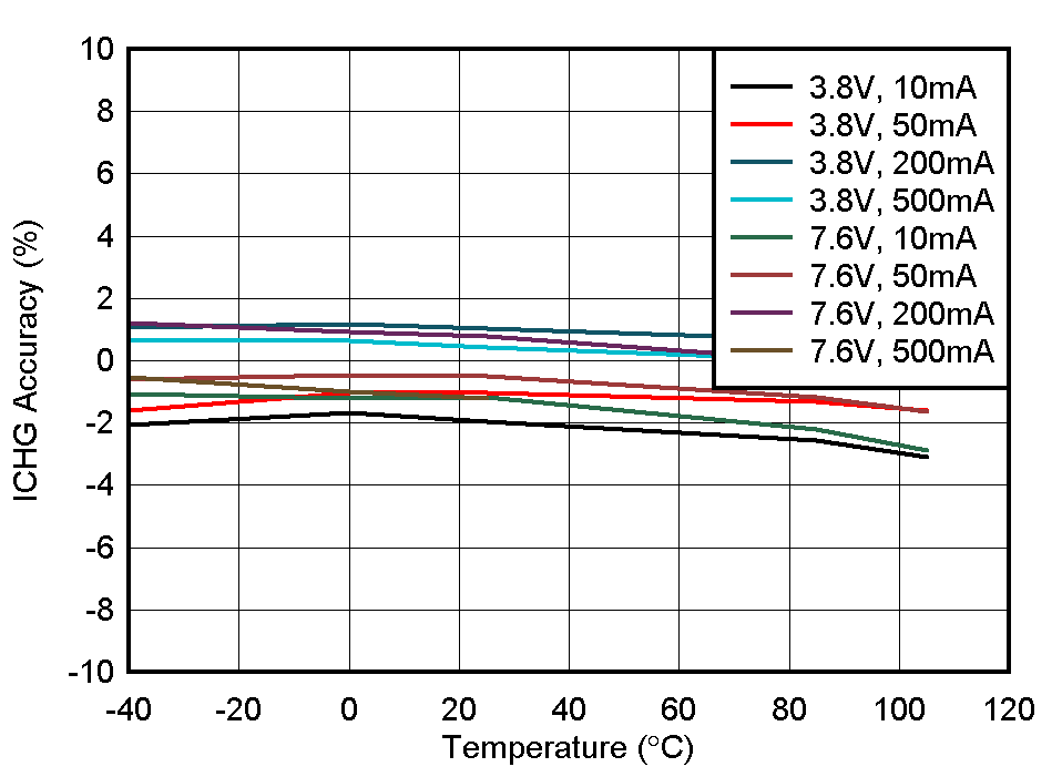
VIN = 5 V and 12 VVOUT = 3.8 V and 7.6 V
Figure 6-5 ICHG Accuracy vs. Temperature
GUID-20200827-CA0I-DRZQ-ZTZX-SWBTTG9XXW6J-low.gif
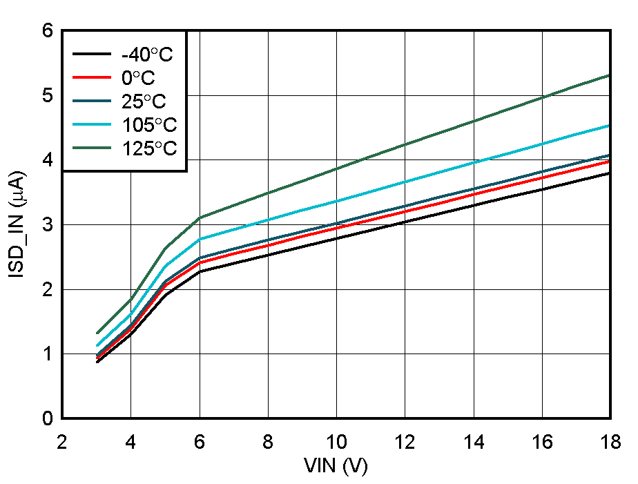
CE Pin = HIGHVOUT = 0 V
Figure 6-7 Input Shutdown Current vs. Input Voltage
GUID-20200827-CA0I-PN2D-VGR1-9BDCX3L7M49F-low.gif
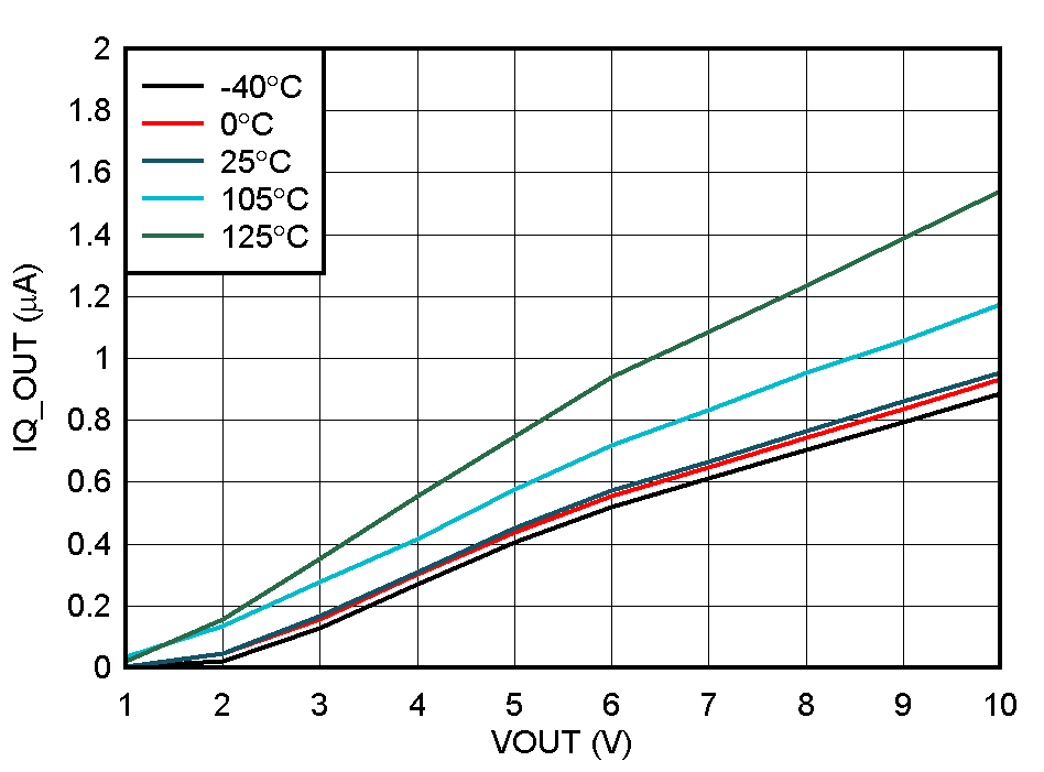
VIN = 0 V
Figure 6-9 Output Quiescent Current vs. Output Voltage
GUID-D804DCE1-AE94-4C35-8135-166DD4139C62-low.gif
IOUT = 10 mAVOUT = 8.4 V
Figure 6-2 Line Regulation
GUID-20200827-CA0I-DVBB-RRN5-MZBDWF99G5DW-low.gif
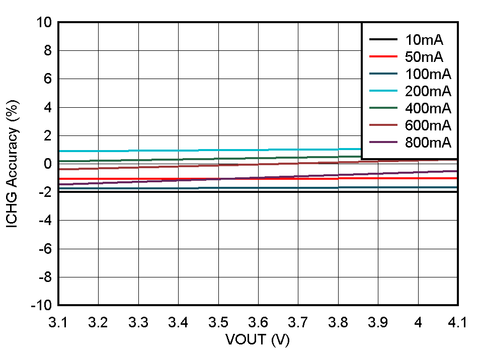
VIN = 5 VTemp. = 25ºC
Figure 6-4 ICHG Accuracy vs. VOUT
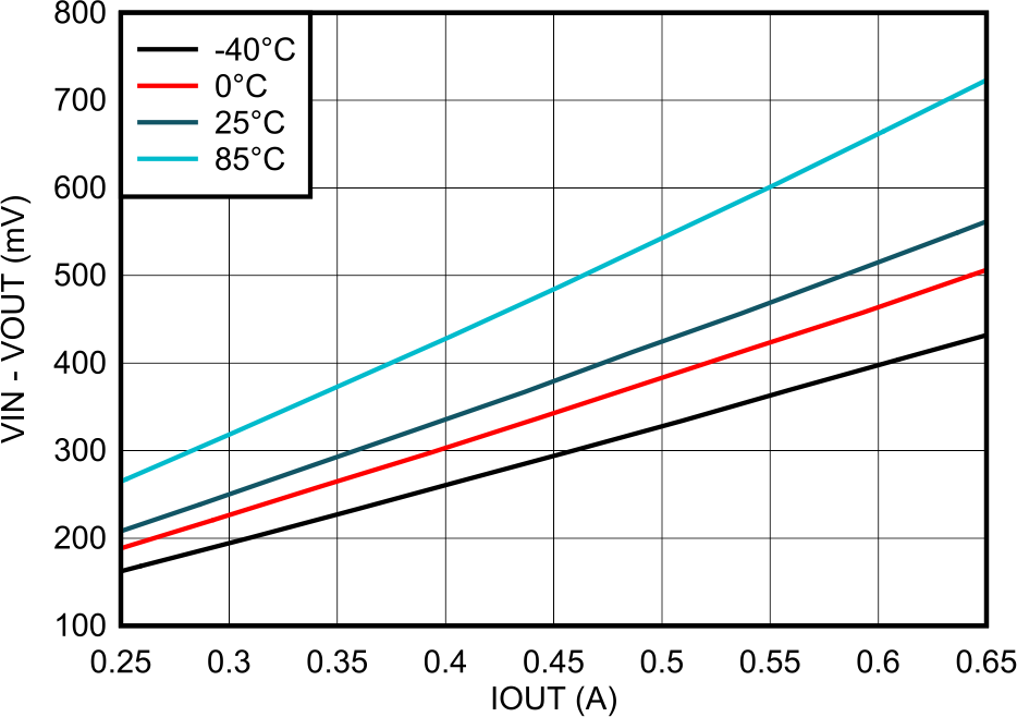
GUID-20211006-SS0I-NSBD-NS9L-3HXJZGNSFFS7-low.pngFigure 6-6 Dropout Voltage vs. Output Current
GUID-20200827-CA0I-PPP7-HZK9-PXVHM9XNL3B7-low.gif
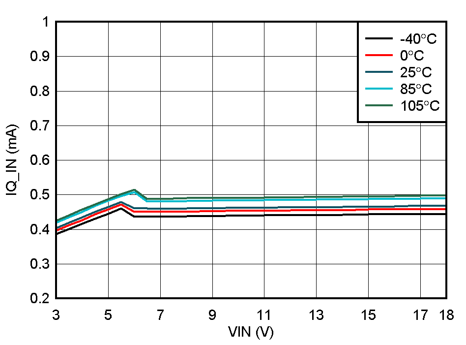
CE Pin = LOWICHG = 0 A
Figure 6-8 Input Quiescent Current vs. Input Voltage