JAJSM15A June 2021 – September 2021 BQ25175
PRODUCTION DATA
- 1 特長
- 2 アプリケーション
- 3 概要
- 4 Revision History
- 5 Pin Configuration and Functions
- 6 Specifications
- 7 Detailed Description
- 8 Application and Implementation
- 9 Power Supply Recommendations
- 10Layout
- 11Device and Documentation Support
- 12Mechanical, Packaging, and Orderable Information
5 Pin Configuration and Functions

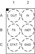
Top View = Xray through a soldered down
part with A1 starting in upper left corner
Figure 5-1 YBG
Package6-Pin DSBGATop ViewTable 5-1 Pin Functions
| PIN | I/O | DESCRIPTION | |
|---|---|---|---|
| NAME | NO. | ||
| OUT | A1 | P | Battery connection. System load may be connected in parallel to battery. Bypass OUT with at least a 1-μF capacitor to GND, place close to the IC. |
| IN | A2 | P | Input power, connected to external DC supply. Bypass IN with at least a 1-μF capacitor to GND, place close to the IC. |
| TS | B1 | I | Temperature qualification voltage input. Connect a negative temperature coefficient (NTC) thermistor directly from TS to GND (AT103-2 recommended). Charge suspends when TS < VHOT or TS > VCOLD. Charge at 20% of ISET when VCOLD > TS > VCOOL. If TS function is not needed, connect an external 10-kΩ resistor from this pin to GND. Pulling TS < VTS_ENZ disables the charger. |
| ISET | B2 | I | Programs the device fast-charge current. An external resistor from ISET to GND defines fast charge current value. Expected range is 30 kΩ (10 mA) to 375 Ω (800 mA). ICHG = KISET / RISET. Precharge current is defined as 20% of ICHG. Termination current is defined as 10% of ICHG. |
| STAT | C1 | O | Open drain charger status indication output. Connect
to pull-up rail via 10-kΩ resistor. LOW indicates charge in progress. HIGH indicates charge complete or charge disabled. When a fault condition is detected, the STAT pin blinks at 1 Hz. If unsued, this pin can be left floating. |
| GND | C2 | – | Ground pin |