JAJSFS8B July   2018  – February 2022 BQ25601D

PRODUCTION DATA  

  1. 特長
  2. アプリケーション
  3. 説明
  4. Revision History
  5. 概要 (続き)
  6. Device Comparison Table
  7. Pin Configuration and Functions
  8. Specifications
    1. 8.1 Absolute Maximum Ratings
    2. 8.2 ESD Ratings
    3. 8.3 Recommended Operating Conditions
    4. 8.4 Thermal information
    5. 8.5 Electrical Characteristics
    6. 8.6 Timing Requirements
    7. 8.7 Typical Characteristics
  9. Detailed Description
    1. 9.1 Overview
    2. 9.2 Functional Block Diagram
    3. 9.3 Feature Description
      1. 9.3.1 Power-On-Reset (POR)
      2. 9.3.2 Device Power Up from Battery without Input Source
      3. 9.3.3 Power Up from Input Source
        1. 9.3.3.1 Power Up REGN Regulation
        2. 9.3.3.2 Poor Source Qualification
        3. 9.3.3.3 Input Source Type Detection
          1. 9.3.3.3.1 D+/D– Detection Sets Input Current Limit in BQ25601D
        4. 9.3.3.4 Input Voltage Limit Threshold Setting (VINDPM Threshold)
        5. 9.3.3.5 Converter Power-Up
      4. 9.3.4 Boost Mode Operation From Battery
      5. 9.3.5 Host Mode and Standalone Power Management
        1. 9.3.5.1 Host Mode and Default Mode in BQ25601D
      6. 9.3.6 Power Path Management
      7. 9.3.7 Battery Charging Management
        1. 9.3.7.1 Autonomous Charging Cycle
        2. 9.3.7.2 Battery Charging Profile
        3. 9.3.7.3 Charging Termination
        4. 9.3.7.4 Thermistor Qualification
        5. 9.3.7.5 JEITA Guideline Compliance During Charging Mode
        6. 9.3.7.6 Boost Mode Thermistor Monitor During Battery Discharge Mode
        7. 9.3.7.7 Charging Safety Timer
    4. 9.4 Device Functional Modes
      1. 9.4.1 Narrow VDC Architecture
      2. 9.4.2 Dynamic Power Management
      3. 9.4.3 Supplement Mode
      4. 9.4.4 Shipping Mode and QON Pin
        1. 9.4.4.1 BATFET Disable Mode (Shipping Mode)
        2. 9.4.4.2 BATFET Enable (Exit Shipping Mode)
        3. 9.4.4.3 BATFET Full System Reset
        4. 9.4.4.4 QON Pin Operations
      5. 9.4.5 Status Outputs ( PG, STAT, INT )
        1. 9.4.5.1 Power Good Indicator ( PGPin PG_STAT Bit)
        2. 9.4.5.2 Charging Status indicator (STAT)
        3. 9.4.5.3 Interrupt to Host ( INT)
    5. 9.5 Protections
      1. 9.5.1 Voltage and Current Monitoring in Converter Operation
        1. 9.5.1.1 Voltage and Current Monitoring in Buck Mode
          1. 9.5.1.1.1 Input Overvoltage (ACOV)
          2. 9.5.1.1.2 System Overvoltage Protection (SYSOVP)
      2. 9.5.2 Voltage and Current Monitoring in Boost Mode
        1. 9.5.2.1 VBUS Soft Start
        2. 9.5.2.2 VBUS Output Protection
        3. 9.5.2.3 Boost Mode Overvoltage Protection
      3. 9.5.3 Thermal Regulation and Thermal Shutdown
        1. 9.5.3.1 Thermal Protection in Buck Mode
        2. 9.5.3.2 Thermal Protection in Boost Mode
      4. 9.5.4 Battery Protection
        1. 9.5.4.1 Battery Overvoltage Protection (BATOVP)
        2. 9.5.4.2 Battery Over-Discharge Protection
        3. 9.5.4.3 System Over-Current Protection
    6. 9.6 Programming
      1. 9.6.1 Serial Interface
        1. 9.6.1.1 Data Validity
        2. 9.6.1.2 START and STOP Conditions
        3. 9.6.1.3 Byte Format
        4. 9.6.1.4 Acknowledge (ACK) and Not Acknowledge (NACK)
        5. 9.6.1.5 Slave Address and Data Direction Bit
        6. 9.6.1.6 Single Read and Write
        7. 9.6.1.7 Multi-Read and Multi-Write
    7. 9.7 Register Maps
      1. 9.7.1  REG00 (address = 00) [reset = 00010111]
      2. 9.7.2  REG01 (address = 01) [reset = 00011010]
      3. 9.7.3  REG02 (address = 02) [reset = 10100 010]
      4. 9.7.4  REG03 (address = 03) [reset = 001 0001 0]
      5. 9.7.5  REG04 (address = 04) [reset = 01011000]
      6. 9.7.6  REG05 (address = 05) [reset = 10011111]
      7. 9.7.7  REG06 (address = 06) [reset = 01100110]
      8. 9.7.8  REG07 (address = 07) [reset = 01001100]
      9. 9.7.9  REG08 (address = 08) [reset = xxxxxxxx]
      10. 9.7.10 REG09 (address = 09) [reset = xxxxxxxx]
      11. 9.7.11 REG0A (address = 0A) [reset = xxxxxx00]
      12. 9.7.12 REG0B (address = 0B) [reset = 00111xxx]
  10. 10Layout
    1. 10.1 Layout Guidelines
    2. 10.2 Layout Example
  11. 11Device and Documentation Support
    1. 11.1 Device Support
      1. 11.1.1 Third-Party Products Disclaimer
    2. 11.2 Documentation Support
      1. 11.2.1 Related Documentation
    3. 11.3 Receiving Notification of Documentation Updates
    4. 11.4 サポート・リソース
    5. 11.5 Trademarks
    6. 11.6 Electrostatic Discharge Caution
    7. 11.7 Glossary

パッケージ・オプション

メカニカル・データ(パッケージ|ピン)
サーマルパッド・メカニカル・データ
発注情報

JEITA Guideline Compliance During Charging Mode

To improve the safety of charging Li-ion batteries, JEITA guideline was released on April 20, 2007. The guideline emphasized the importance of avoiding a high charge current and high charge voltage at certain low and high temperature ranges.

To initiate a charge cycle, the voltage on TS pin must be within the VT1 to VT5 thresholds. If TS voltage exceeds the T1-T5 range, the controller suspends charging and waits until the battery temperature is within the T1 to T5 range.

At cool temperature (T1-T2), JEITA recommends the charge current to be reduced to half of the charge current or lower. At warm temperature (T3-T5), JEITA recommends charge voltage less than 4.1 V charge termination is disabled for cool and warm conditions.

The charger provides flexible voltage/current settings beyond the JEITA requirement. The voltage setting at warm temperature (T3-T5) can be VREG or 4.1V (configured by JEITA_VSET). The current setting at cool temperature (T1-T2) can be further reduced to 20% of fast charge current (JEITA_ISET).

GUID-A2CB40BE-04D4-4B6E-818C-48CB28C186F1-low.gifFigure 9-3 JEITA Profile: Charging Current
GUID-D3E07C7A-9CA8-4929-A784-3D389F13D90B-low.gifFigure 9-4 JEITA Profile: Charging Voltage
GUID-20201208-CA0I-3MLS-RZCM-PD7MTMZ95WV9-low.gif Figure 9-5 TS Resistor Network

Equation 1 through Equation 2 describe updates to the resistor bias network.

Equation 1. GUID-4996A072-DE3A-4952-82F7-B673BB19EF92-low.gif
Equation 2. GUID-E203F083-363C-4417-84F4-AB1050CB31E5-low.gif

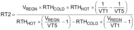
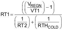
Select 0°C to 60°C range for Li-ion or Li-polymer battery:

  • RTHCOLD = 27.28 KΩ
  • RTHHOT = 3.02 KΩ
  • RT1 = 5.23 KΩ
  • RT2 = 30.9 KΩ