SWRS116F August 2011 – October 2014 CC1175
PRODUCTION DATA.
- 1 Device Overview
- 2Revision History
- 3Terminal Configuration and Functions
-
4Specifications
- 4.1 Absolute Maximum Ratings
- 4.2 Handling Ratings
- 4.3 Recommended Operating Conditions (General Characteristics)
- 4.4 Thermal Resistance Characteristics for RHB Package
- 4.5 RF Characteristics
- 4.6 Regulatory Standards
- 4.7 Current Consumption, Static Modes
- 4.8 Current Consumption, Transmit Modes
- 4.9 Transmit Parameters
- 4.10 PLL Parameters
- 4.11 Wake-up and Timing
- 4.12 High-Speed Crystal Oscillator
- 4.13 High-Speed Clock Input (TCXO)data to TCXO table
- 4.14 32-kHz Clock Input
- 4.15 Low-Speed RC Oscillator
- 4.16 I/O and Reset
- 4.17 Temperature Sensor
- 4.18 Typical Characteristics
- 5Detailed Description
- 6Typical Application Circuit
- 7Device and Documentation Support
- 8Mechanical Packaging and Orderable Information
パッケージ・オプション
メカニカル・データ(パッケージ|ピン)
- RHB|32
サーマルパッド・メカニカル・データ
- RHB|32
発注情報
5 Detailed Description
5.1 Block Diagram
Figure 5-1 shows the system block diagram of the CC1175 device.
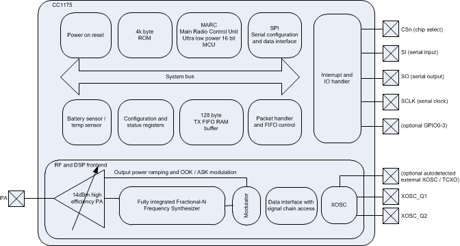 Figure 5-1 System Block Diagram
5.2 Frequency Synthesizer
At the center of the CC1175 device there is a fully integrated, fractional-N, ultra-high-performance frequency synthesizer. The frequency synthesizer is designed for excellent phase noise performance. The system is designed to comply with the most stringent regulatory spectral masks at maximum transmit power.
Either a crystal can be connected to XOSC_Q1 and XOSC_Q2, or a TCXO can be connected to the EXT_XOSC input. The oscillator generates the reference frequency for the synthesizer, as well as clocks for the digital part. If a TCXO is used, the CC1175 device automatically turns on and off the TCXO when needed to support low-power modes.
5.3 Transmitter
The CC1175 transmitter is based on direct synthesis of the RF frequency (in-loop modulation). To achieve effective spectrum usage, the CC1175 device has extensive data filtering and shaping in TX mode to support high throughput data communication in narrowband channels. The modulator also controls power ramping to remove issues such as spectral splattering when driving external high-power RF amplifiers.
The modulator also controls the PA power level to support on/off keying (OOK) and amplitude shift keying (ASK).
5.4 Radio Control and User Interface
The CC1175 digital control system is built around the main radio control (MARC), which is implemented using an internal high-performance, 16-bit ultra-low-power processor. MARC handles power modes, radio sequencing, and protocol timing.
A 4-wire SPI serial interface is used for configuration and data buffer access. The digital baseband includes support for channel configuration, packet handling, and data buffering. The host MCU can stay in power-down mode until a valid RF packet is received. This greatly reduces power consumption. When the host MCU receives a valid RF packet, it burst-reads the data. This reduces the required computing power.
The CC1175 radio control and user interface are based on the widely used CC1101 transceiver. This relationship enables an easy transition between the two platforms. The command strobes and the main radio states are the same for the two platforms.
For legacy formats, the CC1175 device also supports two serial modes.
- Synchronous serial mode: The CC1175 device provides the MCU with a bit clock for sampling input data.
- Transparent mode: The CC1175 device samples the input pin at a configurable rate.
5.5 Low-Power and High-Performance Modes
The CC1175 device is highly configurable, enabling trade-offs between power and performance to be made based on the needs of the application. This data sheet describes two modes, low-power mode and high-performance mode, which represent configurations where the device is optimized for either power or performance.