JAJSQQ5A december   2022  – june 2023 CC1354R10

ADVANCE INFORMATION  

  1.   1
  2. 特長
  3. アプリケーション
  4. 概要
  5. Functional Block Diagram
  6. Revision History
  7. Device Comparison
  8. Terminal Configuration and Functions
    1. 7.1 Pin Diagram – RGZ Package (Top View)
    2. 7.2 Signal Descriptions – RGZ Package
    3. 7.3 Connections for Unused Pins and Modules – RGZ Package
    4. 7.4 Pin Diagram – RSK Package (Top View)
    5. 7.5 Signal Descriptions – RSK Package
    6. 7.6 Connection of Unused Pins and Module – RSK Package
  9. Specifications
    1. 8.1  Absolute Maximum Ratings
    2. 8.2  ESD Ratings
    3. 8.3  Recommended Operating Conditions
    4. 8.4  Power Supply and Modules
    5. 8.5  Power Consumption - Power Modes
    6. 8.6  Power Consumption - Radio Modes
    7. 8.7  Nonvolatile (Flash) Memory Characteristics
    8. 8.8  Thermal Resistance Characteristics
    9. 8.9  RF Frequency Bands
    10. 8.10 861 MHz to 1054 MHz - Receive (RX)
    11. 8.11 861 MHz to 1054 MHz - Transmit (TX) 
    12. 8.12 861 MHz to 1054 MHz - PLL Phase Noise Wideband Mode
    13. 8.13 861 MHz to 1054 MHz - PLL Phase Noise Narrowband Mode
    14. 8.14 Bluetooth Low Energy - Receive (RX)
    15. 8.15 Bluetooth Low Energy - Transmit (TX)
    16. 8.16 Zigbee and Thread - IEEE 802.15.4-2006 2.4 GHz (OQPSK DSSS1:8, 250 kbps) - RX
    17. 8.17 Zigbee and Thread - IEEE 802.15.4-2006 2.4 GHz (OQPSK DSSS1:8, 250 kbps) - TX
    18. 8.18 Timing and Switching Characteristics
      1. 8.18.1 Reset Timing
      2. 8.18.2 Wakeup Timing
      3. 8.18.3 Clock Specifications
        1. 8.18.3.1 48 MHz Clock Input (TCXO)
        2. 8.18.3.2 48 MHz Crystal Oscillator (XOSC_HF)
        3. 8.18.3.3 48 MHz RC Oscillator (RCOSC_HF)
        4. 8.18.3.4 2 MHz RC Oscillator (RCOSC_MF)
        5. 8.18.3.5 32.768 kHz Crystal Oscillator (XOSC_LF)
        6. 8.18.3.6 32 kHz RC Oscillator (RCOSC_LF)
      4. 8.18.4 Serial Peripheral Interface (SPI) Characteristics
        1. 8.18.4.1 SPI Characteristics
        2. 8.18.4.2 SPI Master Mode
        3. 8.18.4.3 SPI Master Mode Timing Diagrams
        4. 8.18.4.4 SPI Slave Mode
        5. 8.18.4.5 SPI Slave Mode Timing Diagrams
      5. 8.18.5 UART
        1. 8.18.5.1 UART Characteristics
    19. 8.19 Peripheral Characteristics
      1. 8.19.1 ADC
        1. 8.19.1.1 Analog-to-Digital Converter (ADC) Characteristics
      2. 8.19.2 DAC
        1. 8.19.2.1 Digital-to-Analog Converter (DAC) Characteristics
      3. 8.19.3 Temperature and Battery Monitor
        1. 8.19.3.1 Temperature Sensor
        2. 8.19.3.2 Battery Monitor
      4. 8.19.4 Comparators
        1. 8.19.4.1 Low-Power Clocked Comparator
        2. 8.19.4.2 Continuous Time Comparator
      5. 8.19.5 Current Source
        1. 8.19.5.1 Programmable Current Source
      6. 8.19.6 GPIO
        1. 8.19.6.1 GPIO DC Characteristics
    20. 8.20 Typical Characteristics
      1. 8.20.1 MCU Current
      2. 8.20.2 RX Current
      3. 8.20.3 TX Current
      4. 8.20.4 RX Performance
      5. 8.20.5 TX Performance
      6. 8.20.6 ADC Performance
  10. Detailed Description
    1. 9.1  Overview
    2. 9.2  System CPU
    3. 9.3  Radio (RF Core)
      1. 9.3.1 Proprietary Radio Formats
      2. 9.3.2 Bluetooth 5.3 Low Energy
      3. 9.3.3 802.15.4 Thread, Zigbee, and 6LoWPAN
    4. 9.4  Memory
    5. 9.5  Sensor Controller
    6. 9.6  Cryptography
    7. 9.7  Timers
    8. 9.8  Serial Peripherals and I/O
    9. 9.9  Battery and Temperature Monitor
    10. 9.10 µDMA
    11. 9.11 Debug
    12. 9.12 Power Management
    13. 9.13 Clock Systems
    14. 9.14 Network Processor
  11. 10Application, Implementation, and Layout
    1. 10.1 Reference Designs
    2. 10.2 Junction Temperature Calculation
  12. 11Device and Documentation Support
    1. 11.1 Tools and Software
      1. 11.1.1 SimpleLink™ Microcontroller Platform
    2. 11.2 Documentation Support
    3. 11.3 サポート・リソース
    4. 11.4 Trademarks
    5. 11.5 静電気放電に関する注意事項
    6. 11.6 用語集
  13. 12Mechanical, Packaging, and Orderable Information
    1. 12.1 Packaging Information

パッケージ・オプション

メカニカル・データ(パッケージ|ピン)
サーマルパッド・メカニカル・データ
発注情報

Packaging Information

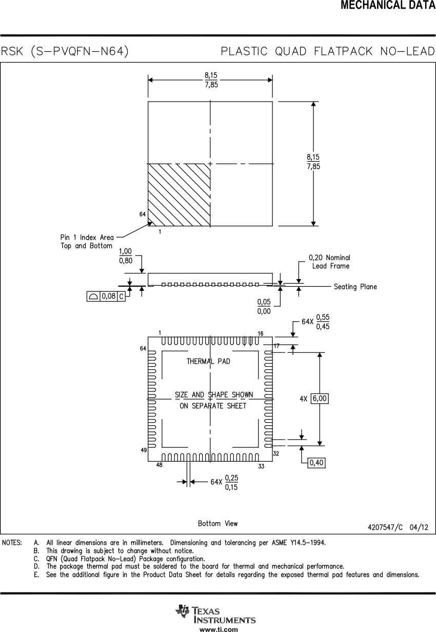
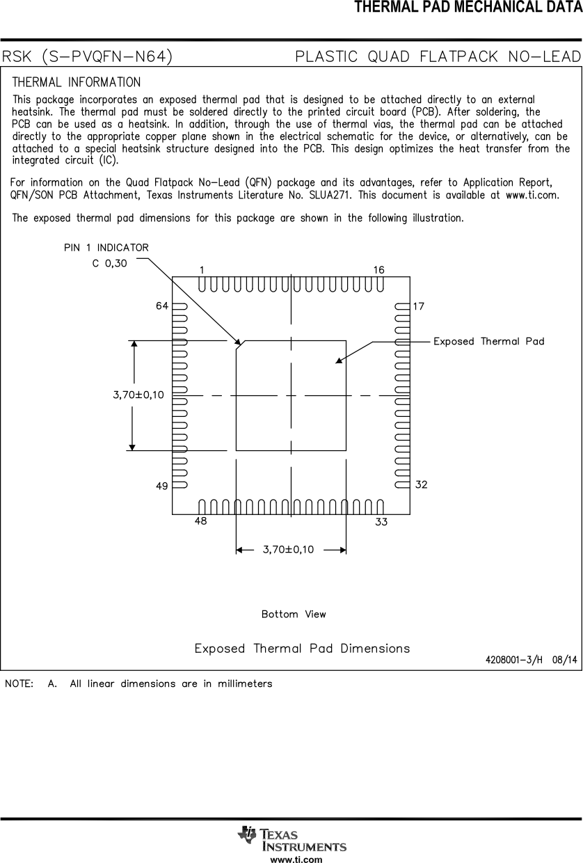
The following pages include mechanical packaging and orderable information. This information is the most current data available for the designated devices. This data is subject to change without notice and revision of this document. For browser-based versions of this data sheet, refer to the left-hand navigation.

Note:

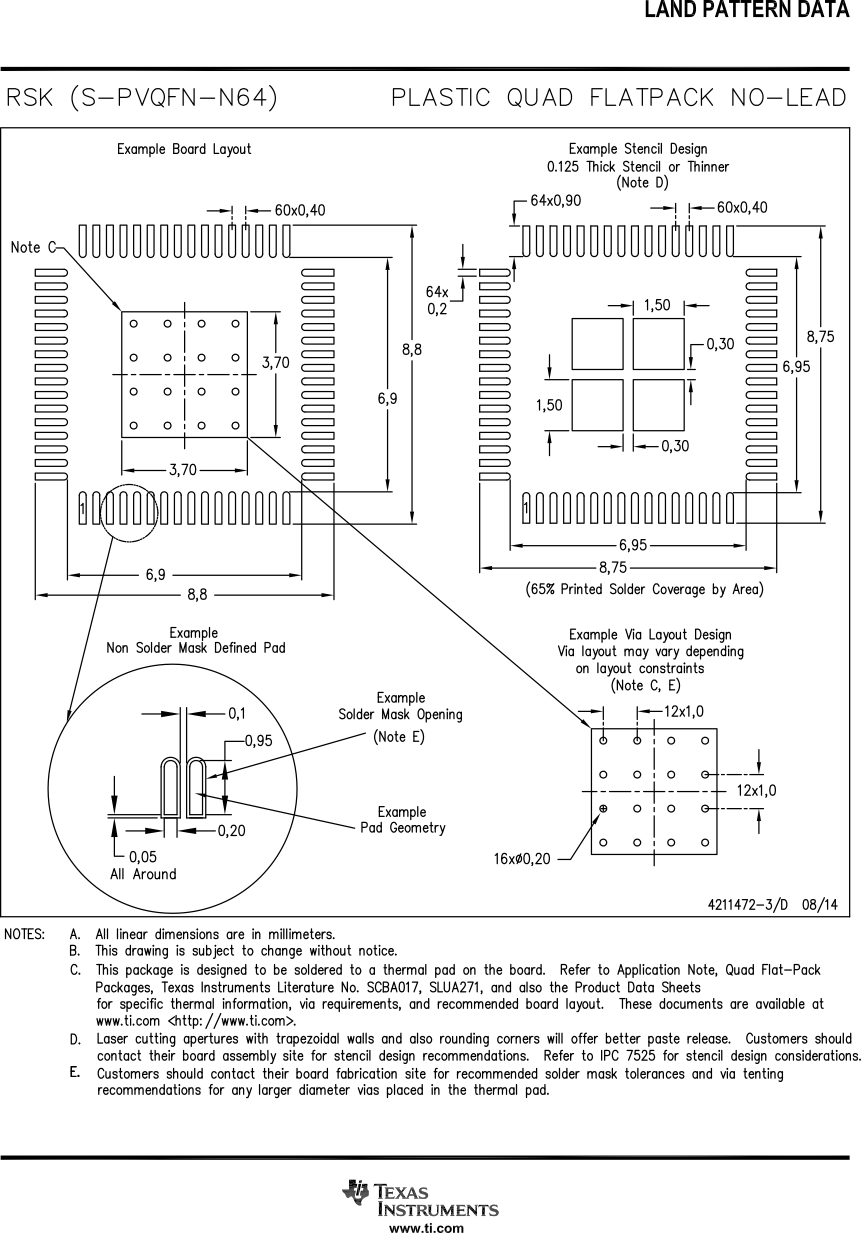
The RSK (S-PQVFN-N64) package drawings in this datasheet are preliminary and will change for the production release of this IC. The change will be related to the exposed thermal pad size of the IC. The current sample has a 3.7 mm x 3.7 mm thermal ground pad. Production devices will have a 4.7 mm x 4.7mm thermal ground pad. It is recommended to design the thermal ground pad to be 4.7 mm x 4.7 mm, with a stencil opening of 3.7 mm x 3.7mm for pre-production devices. For production devices, only the stencil will need to change to 4.7 mm x 4.7 mm. No change to the PCB will be required.

GUID-704CD570-D1CC-4B00-B064-FD159A603EEF-low.gif
GUID-E3E1199C-2B1F-4A9A-A160-607ADC9FCFD7-low.gif
GUID-2F4A0A14-7CED-4585-BF8A-D217016B3410-low.gif
GUID-20210422-CA0I-G7HZ-QSMV-TNHBPBDNDZQ4-low.gif
GUID-20210422-CA0I-TPTD-MDDF-63HMG1MQBBT9-low.gif
GUID-20210422-CA0I-ZT1B-MZMB-QCL2DWNHC5HG-low.gif