SWAS032F July 2013 – February 2015 CC3200
PRODUCTION DATA.
- 1Device Overview
- 2Revision History
- 3Terminal Configuration and Functions
-
4Specifications
- 4.1 Absolute Maximum Ratings
- 4.2 Handling Ratings
- 4.3 Power-On Hours
- 4.4 Recommended Operating Conditions
- 4.5 Brown-Out and Black-Out
- 4.6 Electrical Characteristics (3.3 V, 25°C)
- 4.7 WLAN Receiver Characteristics
- 4.8 WLAN Transmitter Characteristics
- 4.9 Current Consumption
- 4.10 Thermal Characteristics for RGC Package
- 4.11 Timing and Switching Characteristics
- 5Detailed Description
- 6Applications and Implementation
- 7Device and Documentation Support
- 8Mechanical Packaging and Orderable Information
パッケージ・オプション
メカニカル・データ(パッケージ|ピン)
- RGC|64
サーマルパッド・メカニカル・データ
- RGC|64
発注情報
4 Specifications
All measurements are referenced at the device pins, unless otherwise indicated. All specifications are over process and voltage, unless otherwise indicated.
4.1 Absolute Maximum Ratings
over operating free-air temperature range (unless otherwise noted)| PARAMETERS | PINS | MIN | MAX | UNIT |
|---|---|---|---|---|
| VBAT and VIO | 37, 39, 44 | –0.5 | 3.8 | V |
| VIO-VBAT (differential) | 10, 54 | 0.0 | V | |
| Digital inputs | –0.5 | VIO + 0.5 | V | |
| RF pins | –0.5 | 2.1 | V | |
| Analog pins (XTAL) | –0.5 | 2.1 | V | |
| Operating temperature range (TA ) | –40 | +85 | °C |
4.2 Handling Ratings
| MIN | MAX | UNIT | |||
|---|---|---|---|---|---|
| Tstg | Storage temperature range | –55 | +125 | °C | |
| VESD | Electrostatic discharge | Human body model (HBM), per ANSI/ESDA/JEDEC JS-001, all pins(1) | –2000 | +2000 | V |
| Charged device model (CDM), per JEDEC specification JESD22-C101, all pins(2) | –500 | +500 | V | ||
| CONDITIONS | POH | |
|---|---|---|
| TAmbient up to 85°C, assuming 20% active mode and 80% sleep mode | 17,500(1) | |
4.4 Recommended Operating Conditions
over operating free-air temperature range (unless otherwise noted) (1)(4)| PARAMETERS | PINS | CONDITIONS(2)(3) | MIN | TYP | MAX | UNIT |
|---|---|---|---|---|---|---|
| VBAT, VIO (shorted to VBAT) | 10, 37, 39, 44, 54 | Direct battery connection | 2.1 | 3.3 | 3.6 | V |
| VBAT, VIO (shorted to VBAT) | 10, 37, 39, 44, 54 | Preregulated 1.85 V | 1.76 | 1.85 | 1.9 | V |
| Ambient thermal slew | –20 | 20 | °C/minute |
4.5 Brown-Out and Black-Out
The device enters a brown-out condition whenever the input voltage dips below VBROWN (see Figure 4-1 and Figure 4-2). This condition must be considered during design of the power supply routing, especially if operating from a battery. High-current operations (such as a TX packet) cause a dip in the supply voltage, potentially triggering a brown-out. The resistance includes the internal resistance of the battery, contact resistance of the battery holder (4 contacts for a 2 x AA battery) and the wiring and PCB routing resistance.
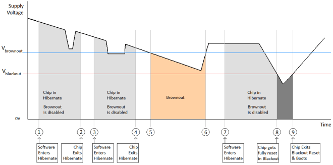 Figure 4-1 Brown-Out and Black-Out Levels (1 of 2)
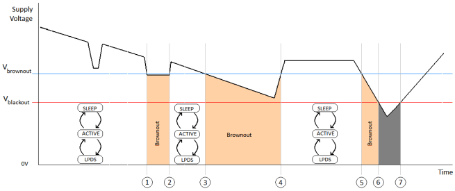 Figure 4-2 Brown-Out and Black-Out Levels (2 of 2)
In the brown-out condition, all sections of the device shut down except for the Hibernate module (including the 32-kHz RTC clock), which remains on. The current in this state can reach approximately 400 µA.
The black-out condition is equivalent to a hardware reset event in which all states within the device are lost.
Table 4-1 lists the brown-out and black-out voltage levels.
Table 4-1 Brown-Out and Black-out Voltage Levels
| CONDITION | VOLTAGE LEVEL | UNIT |
|---|---|---|
| Vbrownout | 2.1 | V |
| Vblackout | 1.67 | V |
4.6 Electrical Characteristics (3.3 V, 25°C)
| GPIO Pins Except 29, 30, 45, 50, 52, and 53 (25°C)(1) | |||||||
|---|---|---|---|---|---|---|---|
| PARAMETER | TEST CONDITIONS | MIN | NOM | MAX | UNIT | ||
| CIN | Pin capacitance | 4 | pF | ||||
| VIH | High-level input voltage | 0.65 × VDD | VDD + 0.5 V | V | |||
| VIL | Low-level input voltage | –0.5 | 0.35 × VDD | V | |||
| IIH | High-level input current | 5 | nA | ||||
| IIL | Low-level input current | 5 | nA | ||||
| VOH | High-level output voltage (VDD = 3.0 V) | 2.4 | V | ||||
| VOL | Low-level output voltage (VDD = 3.0 V) | 0.4 | V | ||||
| IOH | High-level source current, VOH = 2.4 |
2-mA Drive | 2 | mA | |||
| 4-mA Drive | 4 | mA | |||||
| 6-mA Drive | 6 | mA | |||||
| IOL | Low-level sink current, VOL = 0.4 |
2-mA Drive | 2 | mA | |||
| 4-mA Drive | 4 | mA | |||||
| 6-mA Drive | 6 | mA | |||||
| GPIO Pins 29, 30, 45, 50, 52, and 53 (25°C)(1) | |||||||
|---|---|---|---|---|---|---|---|
| PARAMETER | TEST CONDITIONS | MIN | NOM | MAX | UNIT | ||
| CIN | Pin capacitance | 7 | pF | ||||
| VIH | High-level input voltage | 0.65 × VDD | VDD + 0.5V | V | |||
| VIL | Low-level input voltage | –0.5 | 0.35 × VDD | V | |||
| IIH | High-level input current | 50 | nA | ||||
| IIL | Low-level input current | 50 | nA | ||||
| VOH | High-level output voltage (VDD= 3.0 V) |
2.4 | V | ||||
| VOL | Low-level output voltage (VDD= 3.0 V) |
0.4 | V | ||||
| IOH | High-level source current, VOH = 2.4 | 2-mA Drive | 1.5 | mA | |||
| 4-mA Drive | 2.5 | mA | |||||
| 6-mA Drive | 3.5 | mA | |||||
| IOL | Low-level sink current, VOL = 0.4 | 2-mA Drive | 1.5 | mA | |||
| 4-mA Drive | 2.5 | mA | |||||
| 6-mA Drive | 3.5 | mA | |||||
| VIL | nRESET(2) | 0.6 | V | ||||
| Pin Internal Pullup and Pulldown (25°C)(1) | ||||||
|---|---|---|---|---|---|---|
| PARAMETER | TEST CONDITIONS | MIN | NOM | MAX | UNIT | |
| IOH | Pull-Up current, VOH = 2.4 (VDD = 3.0 V) |
5 | 10 | µA | ||
| IOL | Pull-Down current, VOL = 0.4 (VDD = 3.0 V) |
5 | µA | |||
4.7 WLAN Receiver Characteristics
TA = +25°C, VBAT = 2.1 to 3.6 V. Parameters measured at SoC pin on channel 7 (2442 MHz)| Parameter | Condition (Mbps) | Min | Typ | Max | Units |
|---|---|---|---|---|---|
| Sensitivity (8% PER for 11b rates, 10% PER for 11g/11n rates)(10% PER)(2) |
1 DSSS | –95.7 | dBm | ||
| 2 DSSS | –93.6 | ||||
| 11 CCK | –88.0 | ||||
| 6 OFDM | –90.0 | ||||
| 9 OFDM | –89.0 | ||||
| 18 OFDM | –86.0 | ||||
| 36 OFDM | –80.5 | ||||
| 54 OFDM | –74.0 | ||||
| MCS0 (GF)(1) | –89.0 | ||||
| MCS7 (GF)(1) | –71.0 | ||||
| Maximum input level (10% PER) |
802.11b | –4.0 | |||
| 802.11g | –10.0 |
4.8 WLAN Transmitter Characteristics
TA = +25°C, VBAT = 2.1 to 3.6 V. Parameters measured at SoC pin on channel 7 (2442 MHz).(1)| Parameter | Condition(2) | Min | Typ | Max | Units |
|---|---|---|---|---|---|
| Maximum RMS output power measured at 1 dB from IEEE spectral mask or EVM | 1 DSSS | 18.0 | dBm | ||
| 2 DSSS | 18.0 | ||||
| 11 CCK | 18.3 | ||||
| 6 OFDM | 17.3 | ||||
| 9 OFDM | 17.3 | ||||
| 18 OFDM | 17.0 | ||||
| 36 OFDM | 16.0 | ||||
| 54 OFDM | 14.5 | ||||
| MCS7 (MM) | 13.0 | ||||
| Transmit center frequency accuracy | –25 | 25 | ppm |
4.9 Current Consumption
TA = +25°C, VBAT = 3.6 V| PARAMETER | TEST CONDITIONS(1)(6) | MIN | TYP | MAX | UNIT | ||||
|---|---|---|---|---|---|---|---|---|---|
| MCU ACTIVE | NWP ACTIVE | TX | 1 DSSS | TX power level = 0 | 278 | mA | |||
| TX power level = 4 | 194 | ||||||||
| 6 OFDM | TX power level = 0 | 254 | |||||||
| TX power level = 4 | 185 | ||||||||
| 54 OFDM | TX power level = 0 | 229 | |||||||
| TX power level = 4 | 166 | ||||||||
| RX | 1 DSSS | 59 | |||||||
| 54 OFDM | 59 | ||||||||
| NWP idle connected(3) | 15.3 | ||||||||
| MCU SLEEP | NWP ACTIVE | TX | 1 DSSS | TX power level = 0 | 275 | mA | |||
| TX power level = 4 | 191 | ||||||||
| 6 OFDM | TX power level = 0 | 251 | |||||||
| TX power level = 4 | 182 | ||||||||
| 54 OFDM | TX power level = 0 | 226 | |||||||
| TX power level = 4 | 163 | ||||||||
| RX | 1 DSSS | 56 | |||||||
| 54 OFDM | 56 | ||||||||
| NWP idle connected(3) | 12.2 | ||||||||
| MCU LPDS | NWP active | TX | 1 DSSS | TX power level = 0 | 272 | mA | |||
| TX power level = 4 | 188 | ||||||||
| 6 OFDM | TX power level = 0 | 248 | |||||||
| TX power level = 4 | 179 | ||||||||
| 54 OFDM | TX power level = 0 | 223 | |||||||
| TX power level = 4 | 160 | ||||||||
| RX | 1 DSSS | 53 | |||||||
| 54 OFDM | 53 | ||||||||
| NWP LPDS(2) | 0.25 | ||||||||
| NWP idle connected(3) | 0.825 | ||||||||
| MCU hibernate(7) | NWP hibernate(4) | 4 | µA | ||||||
| Peak calibration current (5) | VBAT = 3.3 V | 450 | mA | ||||||
| VBAT = 2.1 V | 670 | ||||||||
| VBAT = 1.85 V | 700 | ||||||||
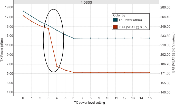
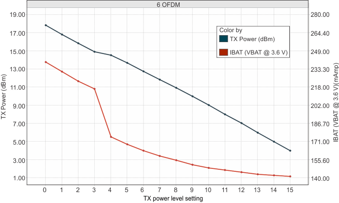 Figure 4-4 TX Power and IBAT vs TX Power Level Settings (6 OFDM)
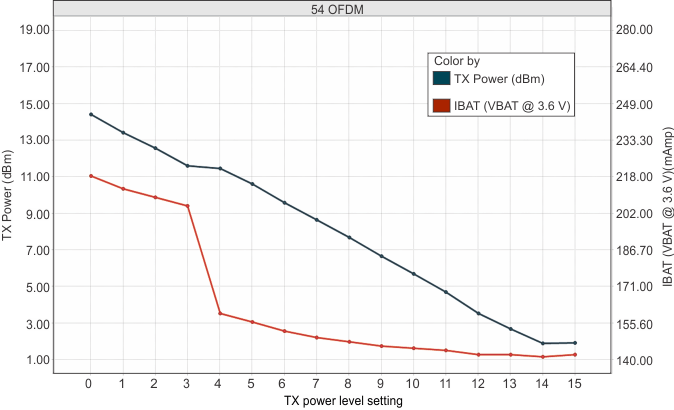 Figure 4-5 TX Power and IBAT vs TX Power Level Settings (54 OFDM)
4.10 Thermal Characteristics for RGC Package
| AIR FLOW | ||||
|---|---|---|---|---|
| PARAMETER | 0 lfm (C/W) | 150 lfm (C/W) | 250 lfm (C/W) | 500 lfm (C/W) |
| θja | 23 | 14.6 | 12.4 | 10.8 |
| Ψjt | 0.2 | 0.2 | 0.3 | 0.1 |
| Ψjb | 2.3 | 2.3 | 2.2 | 2.4 |
| θjc | 6.3 | |||
| θjb | 2.4 | |||
4.11 Timing and Switching Characteristics
4.11.1 Power Supply Sequencing
For proper operation of the CC3200 device, perform the recommended power-up sequencing as follows:
- Tie VBAT (pins 37, 39, 44) and VIO (pins 54 and 10) together on the board.
- Hold the RESET pin low while the supplies are ramping up. TI recommends using a simple RC circuit (100K || 0.1 µF, RC = 10 ms).
- For an external RTC clock, ensure that the clock is stable before RESET is deasserted (high).
For timing diagrams, see Section 4.11.2, Reset Timing.
4.11.2 Reset Timing
4.11.2.1 nRESET (32K XTAL)
Figure 4-6 shows the reset timing diagram for the 32K XTAL first-time power-up and reset removal.
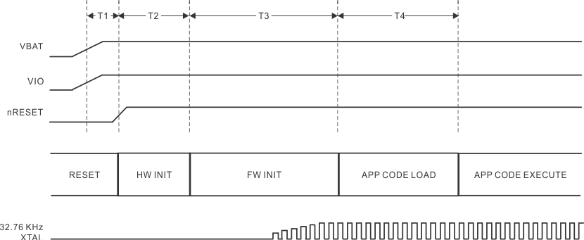 Figure 4-6 First-Time Power-Up and Reset Removal Timing Diagram (32K XTAL)
Table 4-2 describes the timing requirements for the 32K XTAL first-time power-up and reset removal.
Table 4-2 First-Time Power-Up and Reset Removal Timing Requirements (32K XTAL)
| Item | Name | Description | Min | Typ | Max |
|---|---|---|---|---|---|
| T1 | Supply settling time | Depends on application board power supply, decap, and so on | 3 ms | ||
| T2 | Hardware wakeup time | 25 ms | |||
| T3 | Time taken by ROM firmware to initialize hardware | Includes 32.768 -kHz XOSC settling time | 1.1 s | ||
| T4 | App code load time | Image size (KByte) x 0.75 ms |
4.11.2.2 nRESET (External 32K)
Figure 4-7 shows the reset timing diagram for the external 32K first-time power-up and reset removal.
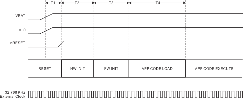 Figure 4-7 First-Time Power-Up and Reset Removal Timing Diagram (External 32K)
Table 4-3 describes the timing requirements for the external 32K first-time power-up and reset removal.
Table 4-3 First-Time Power-Up and Reset Removal Timing Requirements (External 32K)
| Item | Name | Description | Min | Typ | Max |
|---|---|---|---|---|---|
| T1 | Supply settling time | Depends on application board power supply, decap, and so on | 3 ms | ||
| T2 | Hardware wakeup time | 25 ms | |||
| T3 | Time taken by ROM firmware to initialize hardware | Time taken by ROM firmware | 3 ms | ||
| T4 | App code load time | Image size (KByte) x 0.75 ms |
4.11.2.3 Wakeup from Hibernate
Figure 4-8 shows the timing diagram for wakeup from the hibernate state.
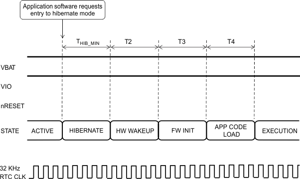
NOTE
The 32.768-kHz XTAL is kept enabled by default when the chip goes to hibernate.
Table 4-4 describes the software hibernate timing requirements.
Table 4-4 Software Hibernate Timing Requirements
| Item | Name | Description | Min | Typ | Max |
|---|---|---|---|---|---|
| Thib_min | Minimum hibernate time | The time for which the device has to be held in hibernate mode | 10 ms | ||
| T2 | Hardware wakeup time | Time taken by the hardware to initialize | 25 ms | ||
| T3 | Firmware initialization time | Time taken by the ROM firmware to initialize the hardware | 3 ms | ||
| T4 | Code download time | Time taken to download the code from the serial flash to on-chip RAM | Image size (KByte) x 0.75 ms | ||
4.11.3 Clock Specifications
The CC3200 device requires two separate clocks for its operation:
- A slow clock running at 32.768 kHz is used for the RTC.
- A fast clock running at 40 MHz is used by the device for the internal processor and the WLAN subsystem.
The device features internal oscillators that enable the use of cheaper crystals rather than dedicated TCXOs for these clocks. The RTC can also be fed externally to provide reuse of an existing clock on the system and reduce overall cost.
4.11.3.1 Slow Clock Using Internal Oscillator
The RTC crystal connected on the device supplies the free-running slow clock. The accuracy of the slow clock frequency must be 32.768 kHz ±150 ppm. In this mode of operation, the crystal is tied between RTC_XTAL_P (pin 51) and RTC_XTAL_N (pin 52) with a suitable load capacitance.
Figure 4-9 shows the crystal connections for the slow clock.
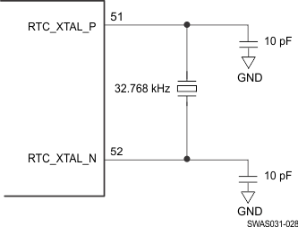 Figure 4-9 RTC Crystal Connections
4.11.3.2 Slow Clock Using an External Clock
When an RTC clock oscillator is present in the system, the CC3200 device can accept this clock directly as an input. The clock is fed on the RTC_XTAL_P line and the RTC_XTAL_N line is held to VIO. The clock must be a CMOS-level clock compatible with VIO fed to the device.
Figure 4-10 shows the external RTC clock input connection.
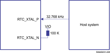 Figure 4-10 External RTC Clock Input
4.11.3.3 Fast Clock (Fref) Using an External Crystal
The CC3200 device also incorporates an internal crystal oscillator to support a crystal-based fast clock. The XTAL is fed directly between WLAN_XTAL_P (pin 23) and WLAN_XTAL_N (pin 22) with suitable loading capacitors.
Figure 4-11 shows the crystal connections for the fast clock.
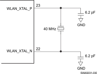 Figure 4-11 Fast Clock Crystal Connections
4.11.3.4 Fast Clock (Fref) Using an External Oscillator
The CC3200 device can accept an external TCXO/XO for the 40-MHz clock. In this mode of operation, the clock is connected to WLAN_XTAL_P (pin 23). WLAN_XTAL_N (pin 22) is connected to GND. The external TCXO/XO can be enabled by TCXO_EN (pin 21) from the device to optimize the power consumption of the system.
If the TCXO does not have an enable input, an external LDO with an enable function can be used. Using the LDO improves noise on the TCXO power supply.
Figure 4-12 shows the connection.
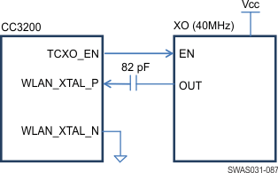 Figure 4-12 External TCXO Input
Table 4-5 lists the external Fref clock requirements.
Table 4-5 External Fref Clock Requirements (–40°C to +85°C)
| Characteristics | Condition | Sym | Min | Typ | Max | Unit | |
|---|---|---|---|---|---|---|---|
| Frequency | 40.00 | MHz | |||||
| Frequency accuracy (Initial + temp + aging) | ±25 | ppm | |||||
| Frequency input duty cycle | 45 | 50 | 55 | % | |||
| Clock voltage limits | Sine or clipped sine wave, AC coupled | Vpp | 0.7 | 1.2 | Vpp | ||
| Phase noise @ 40 MHz | @ 1 kHz | –125 | dBc/Hz | ||||
| @ 10 kHz | –138.5 | dBc/Hz | |||||
| @ 100 kHz | –143 | dBc/Hz | |||||
| Input impedance | Resistance | 12 | KΩ | ||||
| Capacitance | 7 | pF | |||||
4.11.3.5 Input Clocks/Oscillators
Table 4-6 lists the RTC crystal requirements.
Table 4-6 RTC Crystal Requirements
| CHARACTERISTICS | CONDITION | SYM | MIN | TYP | MAX | UNIT |
|---|---|---|---|---|---|---|
| Frequency | 32.768 | kHz | ||||
| Frequency accuracy | Initial + temp + aging | ±150 | ppm | |||
| Crystal ESR | 32.768 kHz, C1 = C2 = 10 pF | 70 | kΩ |
Table 4-7 lists the external RTC digital clock requirements.
Table 4-7 External RTC Digital Clock Requirements
| CHARACTERISTICS | CONDITION | SYM | MIN | TYP | MAX | UNIT |
|---|---|---|---|---|---|---|
| Frequency | 32768 | Hz | ||||
| Frequency accuracy | ±150 | ppm | ||||
| (Initial + temp + aging) | ||||||
| Input transition time tr/tf (10% to 90%) | tr/tf | 100 | ns | |||
| Frequency input duty cycle | 20 | 50 | 80 | % | ||
| Slow clock input voltage limits | Square wave, DC coupled | Vih | 0.65 × VIO | VIO | V | |
| Vil | 0 | 0.35 × VIO | V peak | |||
| Input impedance | 1 | MΩ | ||||
| 5 | pF |
Table 4-8 lists the WLAN fast-clock crystal requirements.
Table 4-8 WLAN Fast-Clock Crystal Requirements
| CHARACTERISTICS | CONDITION | SYM | MIN | TYP | MAX | UNIT |
|---|---|---|---|---|---|---|
| Frequency | 40 | MHz | ||||
| Frequency accuracy | Initial + temp + aging | ±25 | ppm | |||
| Crystal ESR | 40 MHz, C1 = C2 = 6.2 pF | 40 | 50 | 60 | Ohm |
4.11.3.6 WLAN Filter Requirements
The device requires an external bandpass filter to meet the various emission standards, including FCC. Table 4-9 presents the attenuation requirements for the bandpass filter. TI recommends using the same filter used in the reference design to ease the process of certification.
Table 4-9 WLAN Filter Requirements
| Parameter | Frequency (MHz) | Requirements | |||
|---|---|---|---|---|---|
| Min | Typ | Max | Units | ||
| Return loss | 2412 to 2484 | 10 | dB | ||
| Insertion loss(1) | 2412 to 2484 | 1 | 1.5 | dB | |
| Attenuation | 800 to 830 | 30 | 45 | dB | |
| 1600 to 1670 | 20 | 25 | |||
| 3200 to 3300 | 30 | 48 | |||
| 4000 to 4150 | 45 | 50 | |||
| 4800 to 5000 | 20 | 25 | |||
| 5600 to 5800 | 20 | 25 | |||
| 6400 to 6600 | 20 | 35 | |||
| 7200 to 7500 | 35 | 45 | |||
| 7500 to 10000 | 20 | 25 | |||
| Reference Impendence | 2412 to 2484 | 50 | Ω | ||
| Filter type | Bandpass | ||||
4.11.4 Peripherals
This section describes the peripherals that are supported by the CC3200 device:
- SPI
- McASP
- GPIO
- I2C
- IEEE 1149.1 JTAG
- ADC
- Camera parallel port
- UART
4.11.4.1 SPI
4.11.4.1.1 SPI Master
The CC3200 microcontroller includes one SPI module, which can be configured as a master or slave device. The SPI includes a serial clock with programmable frequency, polarity, and phase, a programmable timing control between chip select and external clock generation, and a programmable delay before the first SPI word is transmitted. Slave mode does not include a dead cycle between two successive words.
Figure 4-13 shows the timing diagram for the SPI master.
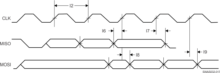 Figure 4-13 SPI Master Timing Diagram
Table 4-10 lists the timing parameters for the SPI master.
Table 4-10 SPI Master Timing Parameters
| Parameter Number | Parameter(1) | Parameter Name | Min | Max | Unit |
|---|---|---|---|---|---|
| I1 | F | Clock frequency | 20 | MHz | |
| I2 | Tclk | Clock period | 50 | ns | |
| I5 | D | Duty cycle | 45 | 55 | % |
| I6 | tIS | RX data setup time | 1 | ns | |
| I7 | tIH | RX data hold time | 2 | ns | |
| I8 | tOD | TX data output delay | 8.5 | ns | |
| I9 | tOH | TX data hold time | 8 | ns |
4.11.4.1.2 SPI Slave
Figure 4-14 shows the timing diagram for the SPI slave.
Figure 4-14 SPI Slave Timing Diagram
Table 4-11 lists the timing parameters for the SPI slave.
Table 4-11 SPI Slave Timing Parameters
| Parameter Number | Parameter(1) | Parameter Name | Min | Max | Unit |
|---|---|---|---|---|---|
| I1 | F | Clock frequency @ VBAT = 3.3 V | 20 | MHz | |
| Clock frequency @ VBAT ≤ 2.1 V | 12 | ||||
| I2 | Tclk | Clock period | 50 | ns | |
| I5 | D | Duty cycle | 45 | 55 | % |
| I6 | tIS | RX data setup time | 4 | ns | |
| I7 | tIH | RX data hold time | 4 | ns | |
| I8 | tOD | TX data output delay | 20 | ||
| I9 | tOH | TX data hold time | 24 | ns |
4.11.4.2 McASP
The McASP interface functions as a general-purpose audio serial port optimized for multichannel audio applications and supports transfer of two stereo channels over two data pins. The McASP consists of transmit and receive sections that operate synchronously and have programmable clock and frame-sync polarity. A fractional divider is available for bit-clock generation.
4.11.4.2.1 I2S Transmit Mode
Figure 4-15 shows the timing diagram for the I2S transmit mode.
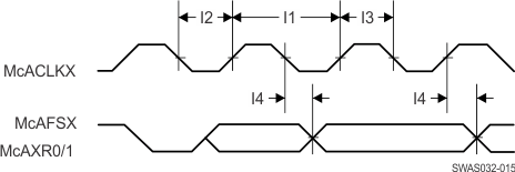 Figure 4-15 I2S Transmit Mode Timing Diagram
Table 4-12 lists the timing parameters for the I2S transmit mode.
Table 4-12 I2S Transmit Mode Timing Parameters
| Parameter Number | Parameter(1) | Parameter Name | Min | Max | Unit |
|---|---|---|---|---|---|
| I1 | fclk | Clock frequency | 9.216 | MHz | |
| I2 | tLP | Clock low period | 1/2 fclk | ns | |
| I3 | tHT | Clock high period | 1/2 fclk | ns | |
| I4 | tOH | TX data hold time | 22 | ns |
4.11.4.2.2 I2S Receive Mode
Figure 4-16 shows the timing diagram for the I2S receive mode.
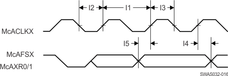 Figure 4-16 I2S Receive Mode Timing Diagram
Table 4-13 lists the timing parameters for the I2S receive mode.
Table 4-13 I2S Receive Mode Timing Parameters
| Parameter Number | Parameter(1) | Parameter Name | Min | Max | Unit |
|---|---|---|---|---|---|
| I1 | fclk | Clock frequency | 9.216 | MHz | |
| I2 | tLP | Clock low period | 1/2 fclk | ns | |
| I3 | tHT | Clock high period | 1/2 fclk | ns | |
| I4 | tOH | RX data hold time | 0 | ns | |
| I5 | tOS | RX data setup time | 15 | ns |
4.11.4.3 GPIO
All digital pins of the device can be used as general-purpose input/output (GPIO) pins.The GPIO module consists of four GPIO blocks, each of which provides eight GPIOs. The GPIO module supports 24 programmable GPIO pins, depending on the peripheral used. Each GPIO has configurable pullup and pulldown strength (weak 10 µA), configurable drive strength (2, 4, and 6 mA), and open-drain enable.
Figure 4-17 shows the GPIO timing diagram.
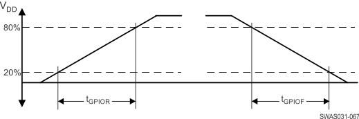 Figure 4-17 GPIO Timing
4.11.4.3.1 GPIO Output Transition Time Parameters (Vsupply = 3.3 V)
Table 4-14 lists the GPIO output transition times for Vsupply = 3.3 V.
Table 4-14 GPIO Output Transition Times (Vsupply = 3.3 V)(1)(2)
| Drive Strength (mA) | Drive Strength Control Bits | Tr (ns) | Tf (ns) | ||||
|---|---|---|---|---|---|---|---|
| Min | Nom | Max | Min | Nom | Max | ||
| 2 | 2MA_EN=1 | 8.0 | 9.3 | 10.7 | 8.2 | 9.5 | 11.0 |
| 4MA_EN=0 | |||||||
| 8MA_EN=0 | |||||||
| 4 | 2MA_EN=0 | 6.6 | 7.1 | 7.6 | 4.7 | 5.2 | 5.8 |
| 4MA_EN=1 | |||||||
| 8MA_EN=0 | |||||||
| 8 | 2MA_EN=0 | 3.2 | 3.5 | 3.7 | 2.3 | 2.6 | 2.9 |
| 4MA_EN=0 | |||||||
| 8MA_EN=1 | |||||||
| 14 | 2MA_EN=1 | 1.7 | 1.9 | 2.0 | 1.3 | 1.5 | 1.6 |
| 4MA_EN=1 | |||||||
| 8MA_EN=1 | |||||||
4.11.4.3.2 GPIO Output Transition Time Parameters (Vsupply = 1.8 V)
Table 4-15 lists the GPIO output transition times for Vsupply = 1.8 V.
Table 4-15 GPIO Output Transition Times (Vsupply = 1.8 V)(1)(2)
| Drive Strength (mA) | Drive Strength Control Bits | Tr (ns) | Tf (ns) | ||||
|---|---|---|---|---|---|---|---|
| Min | Nom | Max | Min | Nom | Max | ||
| 2 | 2MA_EN=1 | 11.7 | 13.9 | 16.3 | 11.5 | 13.9 | 16.7 |
| 4MA_EN=0 | |||||||
| 8MA_EN=0 | |||||||
| 4 | 2MA_EN=0 | 13.7 | 15.6 | 18.0 | 9.9 | 11.6 | 13.6 |
| 4MA_EN=1 | |||||||
| 8MA_EN=0 | |||||||
| 8 | 2MA_EN=0 | 5.5 | 6.4 | 7.4 | 3.8 | 4.7 | 5.8 |
| 4MA_EN=0 | |||||||
| 8MA_EN=1 | |||||||
| 14 | 2MA_EN=1 | 2.9 | 3.4 | 4.0 | 2.2 | 2.7 | 3.3 |
| 4MA_EN=1 | |||||||
| 8MA_EN=1 | |||||||
4.11.4.3.3 GPIO Input Transition Time Parameters
Table 4-16 lists the input transition time parameters.
Table 4-16 GPIO Input Transition Time Parameters
| Parameter | Condition | Symbol | Min | Max | Unit |
|---|---|---|---|---|---|
| Input transition time (tr,tf), 10% to 90% | tr | 1 | 3 | ns | |
| tf | 1 | 3 |
4.11.4.4 I2C
The CC3200 microcontroller includes one I2C module operating with standard (100 Kbps) or fast (400 Kbps) transmission speeds.
Figure 4-18 shows the I2C timing diagram.
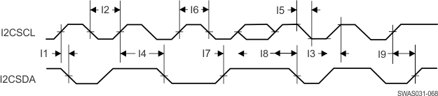 Figure 4-18 I2C Timing
Table 4-17 lists the I2C timing parameters.
Table 4-17 I2C Timing Parameters(3)
| Parameter Number | Parameter | Parameter Name | Min | Max | Unit |
|---|---|---|---|---|---|
| I2 | tLP | Clock low period | See (1). | - | System clock |
| I3 | tSRT | SCL/SDA rise time | – | See (2). | ns |
| I4 | tDH | Data hold time | NA | – | |
| I5 | tSFT | SCL/SDA fall time | – | 3 | ns |
| I6 | tHT | Clock high time | See (1). | – | System clock |
| I7 | tDS | Data setup time | tLP/2 | System clock | |
| I8 | tSCSR | Start condition setup time | 36 | – | System clock |
| I9 | tSCS | Stop condition setup time | 24 | – | System clock |
4.11.4.5 IEEE 1149.1 JTAG
The Joint Test Action Group (JTAG) port is an IEEE standard that defines a test access port (TAP) and boundary scan architecture for digital integrated circuits and provides a standardized serial interface to control the associated test logic. For detailed information on the operation of the JTAG port and TAP controller, see the IEEE Standard 1149.1,Test Access Port and Boundary- Scan Architecture.
Figure 4-19 shows the JTAG timing diagram.
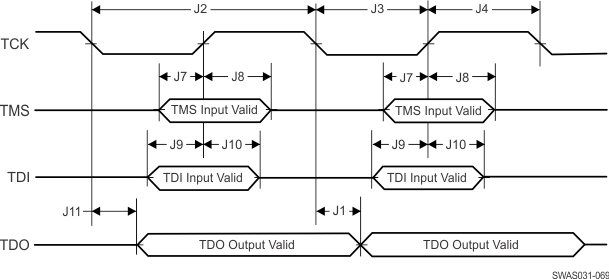 Figure 4-19 JTAG Timing
Table 4-18 lists the JTAG timing parameters.
Table 4-18 JTAG Timing Parameters
4.11.4.6 ADC
Table 4-19 lists the ADC electrical specifications.
Table 4-19 ADC Electrical Specifications
| Parameter | Description | Condition and Assumptions | Min | Typ | Max | Unit |
|---|---|---|---|---|---|---|
| Nbits | Number of bits | 12 | Bits | |||
| INL | Integral nonlinearity | Worst-case deviation from histogram method over full scale (not including first and last three LSB levels) | –2.5 | 2.5 | LSB | |
| DNL | Differential nonlinearity | Worst-case deviation of any step from ideal | –1 | 4 | LSB | |
| Input range | 0 | 1.4 | V | |||
| Driving source impedance | 100 | Ω | ||||
| FCLK | Clock rate | Successive approximation input clock rate | 10 | MHz | ||
| Input capacitance | 3.2 | pF | ||||
| Number of channels | 4 | |||||
| Fsample | Sampling rate of each ADC | 62.5 | KSPS | |||
| F_input_max | Maximum input signal frequency | 31 | kHz | |||
| SINAD | Signal-to-noise and distortion | Input frequency dc to 300 Hz and 1.4 Vpp sine wave input | 55 | 60 | dB | |
| I_active | Active supply current | Average for analog-to-digital during conversion without reference current | 1.5 | mA | ||
| I_PD | Power-down supply current for core supply | Total for analog-to-digital when not active (this must be the SoC level test) | 1 | µA | ||
| Absolute offset error | FCLK = 10 MHz | ±2 | mV | |||
| Gain error | ±2 | % |
Figure 4-20 shows the ADC clock timing diagram.
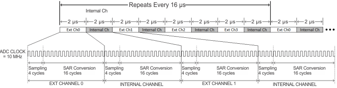 Figure 4-20 ADC Clock Timing
4.11.4.7 Camera Parallel Port
The fast camera parallel port interfaces with a variety of external image sensors, stores the image data in a FIFO, and generates DMA requests. The camera parallel port supports 8 bits.
Figure 4-21 shows the timing diagram for the camera parallel port.
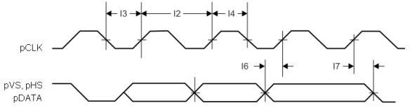 Figure 4-21 Camera Parallel Port Timing Diagram
Table 4-20 lists the timing parameters for the camera parallel port.
Table 4-20 Camera Parallel Port Timing Parameters
| Parameter Number | Parameter | Parameter Name | Min | Max | Unit |
|---|---|---|---|---|---|
| pCLK | Clock frequency | 2 | MHz | ||
| I2 | Tclk | Clock period | 1/pCLK | ns | |
| I3 | tLP | Clock low period | Tclk/2 | ns | |
| I4 | tHT | Clock high period | Tclk/2 | ns | |
| I7 | D | Duty cycle | 45 to 55 | % | |
| I8 | tIS | RX data setup time | 2 | ns | |
| I9 | tIH | RX data hold time | 2 | ns |
4.11.4.8 UART
The CC3200 device includes two UARTs with the following features:
- Programmable baud-rate generator allowing speeds up to 3 Mbps
- Separate 16 x 8 TX and RX FIFOs to reduce CPU interrupt service loading
- Programmable FIFO length, including 1-byte deep operation providing conventional double-buffered interface
- FIFO trigger levels of 1/8, 1/4, 1/2, 3/4, and 7/8
- Standard asynchronous communication bits for start, stop, and parity
- Line-break generation and detection
- Fully programmable serial interface characteristics
- 5, 6, 7, or 8 data bits
- Even, odd, stick, or no-parity bit generation and detection
- 1 or 2 stop-bit generation
- RTS and CTS hardware flow support
- Standard FIFO-level and End-of-Transmission interrupts
- Efficient transfers using μDMA
- Separate channels for transmit and receive
- Receive single request asserted when data is in the FIFO; burst request asserted at programmed FIFO level
- Transmit single request asserted when there is space in the FIFO; burst request asserted at programmed FIFO level
- System clock is used to generate the baud clock.