JAJSHR9B July 2020 – October 2021 CDCE6214-Q1
PRODUCTION DATA
- 1 特長
- 2 アプリケーション
- 3 概要
- 4 Revision History
- 5 概要 (続き)
- 6 Pin Configuration and Functions
-
7 Specifications
- 7.1 Absolute Maximum Ratings
- 7.2 ESD Ratings
- 7.3 Recommended Operating Conditions
- 7.4 Thermal Information
- 7.5 EEPROM Characteristics
- 7.6 Reference Input, Single-Ended Characteristics
- 7.7 Reference Input, Differential Characteristics
- 7.8 Reference Input, Crystal Mode Characteristics
- 7.9 General-Purpose Input Characteristics
- 7.10 Triple Level Input Characteristics
- 7.11 Logic Output Characteristics
- 7.12 Phase Locked Loop Characteristics
- 7.13 Closed-Loop Output Jitter Characteristics
- 7.14 Input and Output Isolation
- 7.15 Buffer Mode Characteristics
- 7.16 PCIe Spread Spectrum Generator
- 7.17 LVCMOS Output Characteristics
- 7.18 LP-HCSL Output Characteristics
- 7.19 LVDS Output Characteristics
- 7.20 Output Synchronization Characteristics
- 7.21 Power-On Reset Characteristics
- 7.22 I2C-Compatible Serial Interface Characteristics
- 7.23 Timing Requirements, I2C-Compatible Serial Interface
- 7.24 Power Supply Characteristics
- 7.25 Typical Characteristics
- 8 Parameter Measurement Information
- 9 Detailed Description
- 10Application and Implementation
- 11Power Supply Recommendations
- 12Layout
- 13Device and Documentation Support
- 14Mechanical, Packaging, and Orderable Information
パッケージ・オプション
デバイスごとのパッケージ図は、PDF版データシートをご参照ください。
メカニカル・データ(パッケージ|ピン)
- RGE|24
サーマルパッド・メカニカル・データ
発注情報
9.5.1 I2C Serial Interface
The CDCE6214-Q1 ultra-low power clock generator provides an I2C-compatible serial interface for register and EEPROM access. The device is compatible to standard-mode I2C at 100 kHz and the fast-mode I2C at 400-kHz clock frequency.
- In fall-back mode, I2C slave address = 67h.
- In other modes, I2C slave address = 68h (Default).
- The LSB bit of the device can be programmed in the EEPROM. For example, if I2C_A0 is programmed H in Page 0 of EEPROM, setting HW_SW_CTRL=0 would set I2C address as 69h.
- Two devices with EEPROM + 1 device in fall-back mode can be used on the same I2C bus with addresses 67h, 68h and 69h.
Table 9-19 I2C-Compatible Serial Interface, Slave Address Byte (16)(17)
| 7 | 6 | 5 | 4 | 3 | 2 | 1 | 0 |
|---|---|---|---|---|---|---|---|
| Slave Address [6:0] | R/W# Bit | ||||||
Table 9-20 I2C-Compatible Serial Interface, Programmable Slave Address (18)(19)
| A6 | A5 | A4 | A3 | A2 | A1 | A0 | HW_SW_SEL | DESCRIPTION |
|---|---|---|---|---|---|---|---|---|
| 1 | 1 | 0 | 0 | 1 | 1 | 1 | MID | Fall-back Mode |
| 1 | 1 | 0 | 1 | 0 | 0 | I2C_A0 | LOW | EEPROM Page 0 |
| 1 | 1 | 0 | 1 | 0 | 0 | I2C_A0 | HIGH | EEPROM Page 1 |
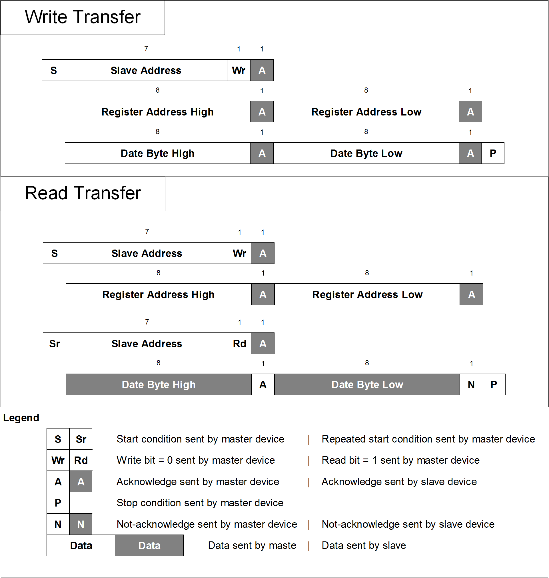
The serial interface uses the following protocol as shown in Figure 9-11. The slave address is followed by a word-wide register offset and a word-wide register value.
 Figure 9-11 I2C-Compatible Serial Interface, Supported Protocol
16. The slave address consists of two sections. The hardwired MSBs A[6:1] and the software-selectable LSBs A[0].
17. The R/W# bit indicates a read (1) or a write (0) transfer.
18. In EEPROM Page 0, Serial Interface is not available. Device configured in Pin Mode
19. In EEPROM Page 1, I2C_A0 is programmed as 0, Expected Slave Address is 68h