SLLSEL1 November 2014 CDCL1810A
PRODUCTION DATA.
- 1 Features
- 2 Applications
- 3 Description
- 4 Simplified Schematic
- 5 Revision History
- 6 Device Comparison Tables
- 7 Pin Configuration and Functions
- 8 Specifications
- 9 Detailed Description
- 10Application and Implementation
- 11Power Supply Recommendations
- 12Layout
- 13Device and Documentation Support
- 14Mechanical, Packaging, and Orderable Information
- 13Mechanical, Packaging, and Orderable Information
パッケージ・オプション
メカニカル・データ(パッケージ|ピン)
- RGZ|48
サーマルパッド・メカニカル・データ
- RGZ|48
発注情報
9 Detailed Description
9.1 Overview
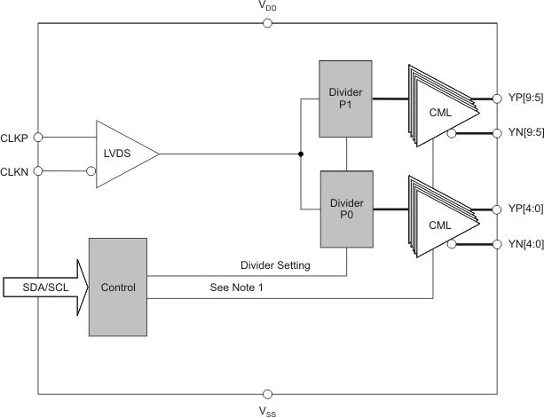
The CDCL1810A is a high performance fanout clock buffer that features two banks of independent integer dividers ranging from 1 to 80. CDCL1810A is designed in a way that individual outputs can be configured -- or reconfigured -- without impacting operation of other outputs.
9.2 Functional Block Diagram
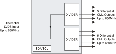 Figure 3. CDCL1810A Simplified Schematic
9.3 Feature Description
9.3.1 Output Enable/Disable
The CDCL1810A does not have an output synchronization feature like the CDCL1810. The CDCL1810A ensures that all outputs stay enabled during any device communication like output enable/disable. Divider changes will apply immediately at the outputs. This may cause a glitch and may result in different phase offsets between both dividers.
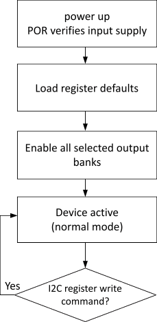 Figure 5. Device Status Flow Chart
9.3.2 SDA/SCL Interface
This section describes the SDA/SCL interface of the CDCL1810A device. The CDCL1810A operates as a slave device of the industry standard 2-pin SDA/SCL bus. It operates in the fast-mode at a bit-rate of up to 400 kbit/s and supports 7-bit addressing compatible with the popular 2-pin serial interface standard.
9.3.2.1 SDA/SCL Bus Slave Device Address
| A6 | A5 | A4 | A3 | A2 | A1 | A0 | R/W |
|---|---|---|---|---|---|---|---|
| 1 | 1 | 0 | 1 | 0 | ADD1 | ADD0 | 0/1 |
The device address is made up of the fixed internal address, 11010 (A6:A2), and configurable external pins ADD1 (A1) and ADD0 (A0). Four different devices with addresses 1101000, 1101001, 1101010 and 1101011, can be addressed via the same SDA/SCL bus interface. The least significant bit of the address byte designates a write or read operation.
R/W Bit:
0 = write to CDCL1810A device
1 = read from CDCL1810A device
9.3.2.2 SDA/SCL Connections Recommendations
The serial interface inputs don’t have glitch suppression circuit. So, any noises or glitches at serial input lines may cause programming error. The serial interface lines should be routed in such a way that the lines would have minimum noise impact from the surroundings.
Figure 6 is recommended to improve the interconnections.
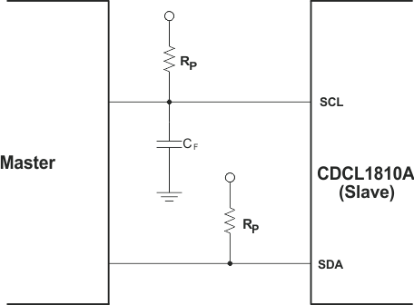 Figure 6. Serial Interface Connections
Lower RP resistor value (around 1 kΩ) should be chosen so that signals will have faster rise time. A capacitor can be connected to SCL line to ground which will act as a filter.
An I2C level translator will help to overcome the noises issue.
9.4 Device Functional Modes
The device is designed to operate from an input voltage supply of 1.8 V. In the default power on reset, all device outputs are enabled and the dividers P0 and P1 are set to 1.
9.5 Programming
9.5.1 SDA/SCL Interface
This section describes the SDA/SCL interface of the DCDL1810A device. The CDCL1810A operates as a slave device of the industry standard 2-pin SDA/SCL bus. It operates in the fast-mode at a bit-rate of up to 400 kb/s and supports 7-bit addressing compatible with the popular 2-pin serial interface standard. The device address is made up of the fixed internal address, 11010 (A6:A2), and configurable external pins ADD1 (A1) and ADD0 (A0). Four different devices with addresses 1101000, 1101001, 1101010, and 1101011, can be addressed via the same SDA/SCL bus interface. The least significant bit of the address byte designates a write or read operation.
R/W bit:
0 = write to CDCL1810 device.
1 = read from CDCL1810 device.
9.5.2 Command Code Definition
Table 3. Command Code Definition
| BIT | DESCRIPTION |
|---|---|
| C7 | 1 = Byte Write / Read or Word Write / Read operation |
| (C6:C0) | Byte Offset for Byte Write / Read and Word Write / Read operation. |
Table 4. SDA/SCL Bus Slave Device Address
| A6 | A5 | A4 | A3 | A2 | A1 | A0 | R/W |
|---|---|---|---|---|---|---|---|
| 1 | 1 | 0 | 1 | 0 | ADD1 | ADD0 | 0/1 |
Table 5. Command Code for Byte Write / Read Operation
| HEX CODE | C7 | C6 | C5 | C4 | C3 | C2 | C1 | C0 | |
|---|---|---|---|---|---|---|---|---|---|
| byte 0 | 80h | 1 | 0 | 0 | 0 | 0 | 0 | 0 | 0 |
| byte 1 | 81h | 1 | 0 | 0 | 0 | 0 | 0 | 0 | 1 |
| byte 2 | 82h | 1 | 0 | 0 | 0 | 0 | 0 | 1 | 0 |
| byte 3 | 83h | 1 | 0 | 0 | 0 | 0 | 0 | 1 | 1 |
| byte 4 | 84h | 1 | 0 | 0 | 0 | 0 | 1 | 0 | 0 |
| byte 5 | 85h | 1 | 0 | 0 | 0 | 0 | 1 | 0 | 1 |
| byte 6 | 86h | 1 | 0 | 0 | 0 | 0 | 1 | 1 | 0 |
Table 6. Command Code for Word Write / Read Operation
| HEX CODE | C7 | C6 | C5 | C4 | C3 | C2 | C1 | C0 | |
|---|---|---|---|---|---|---|---|---|---|
| word 0: byte 0 and byte 1 | 80h | 1 | 0 | 0 | 0 | 0 | 0 | 0 | 0 |
| word 1: byte 1 and byte 2 | 81h | 1 | 0 | 0 | 0 | 0 | 0 | 0 | 1 |
| word 2: byte 2 and byte 3 | 82h | 1 | 0 | 0 | 0 | 0 | 0 | 1 | 0 |
| word 3: byte 3 and byte 4 | 83h | 1 | 0 | 0 | 0 | 0 | 0 | 1 | 1 |
| word 4: byte 4 and byte 5 | 84h | 1 | 0 | 0 | 0 | 0 | 1 | 0 | 0 |
| word 5: byte 5 and byte 6 | 85h | 1 | 0 | 0 | 0 | 0 | 1 | 0 | 1 |
| word 6: byte 6 and byte 7 | 86h | 1 | 0 | 0 | 0 | 0 | 1 | 1 | 0 |
9.5.3 SDA/SCL Timing Characteristics
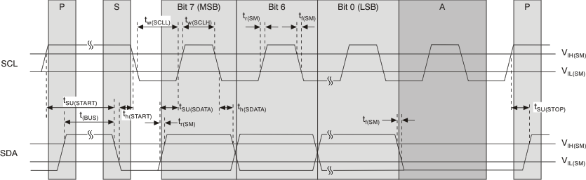 Figure 7. Timing Diagram for the SDA/SCL Serial Control Interface
9.5.4 SDA/SCL Programming Sequence
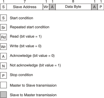 Figure 8. Legend for Programming Sequence
Table 1. Byte WriteProgramming Sequence
| 1 | 7 | 1 | 1 | 8 | 1 | 8 | 1 | 1 |
| S | Slave Address | Wr | A | Command Code | A | Data Byte | A | P |
Table 2. Byte ReadProgramming Sequence
| 1 | 7 | 1 | 1 | 8 | 1 | 1 | 7 | 1 | 1 | 8 | 1 | 1 |
| S | Slave Address | Wr | A | Command Code | A | S | Slave Address | Rd | A | Data Byte | N | P |
Table 3. Word WriteProgramming Sequence:
| 1 | 7 | 1 | 1 | 8 | 1 | 8 | 1 | 8 | 1 | 1 |
| S | Slave Address | Wr | A | Command Code | A | Data Byte Low | A | Data Byte High | A | P |
Table 4. Word ReadProgramming Sequence:
| 1 | 7 | 1 | 1 | 8 | 1 | 1 | 7 | 1 | 1 | 8 | 1 | 8 | 1 | 1 |
| S | Slave Address | Wr | A | Command Code | A | S | Slave Address | Rd | A | Data Byte | A | Data Byte | N | P |
9.6 Register Maps
9.6.1 SDA/SCL Bus Configuration Command Bitmap
9.6.1.1 Byte 0:
| BIT | BIT NAME | DESCRIPTION/FUNCTION | TYPE | POWER UP CONDITION |
REFERENCE TO |
|---|---|---|---|---|---|
| 7 | MANF[7] | Manufacturer reserved | R | ||
| 6 | MANF[6] | Manufacturer reserved | R | ||
| 5 | REV[2] | Device revision | R | 1 | |
| 4 | REV[1] | Device revision | R | 0 | |
| 3 | REV[0] | Device revision | R | 0 | |
| 2 | MANF[2] | Manufacturer reserved | R | ||
| 1 | MANF[1] | Manufacturer reserved | R | ||
| 0 | MANF[0] | Manufacturer reserved | R |
9.6.1.2 Byte 1:
| BIT | BIT NAME | DESCRIPTION/FUNCTION | TYPE | POWER UP CONDITION | REFERENCE TO |
|---|---|---|---|---|---|
| 7 | RES | Reserved | R/W | 0 | |
| 6 | RES | Reserved | R/W | 0 | |
| 5 | RES | Reserved | R/W | 1 | |
| 4 | RES | Reserved | R/W | 0 | |
| 3 | RES | Reserved | R/W | 0 | |
| 2 | RES | Reserved | R/W | 0 | |
| 1 | RES | Reserved | R/W | 0 | |
| 0 | RES | Reserved | R/W | 0 |
9.6.1.3 Byte 2:
| BIT | BIT NAME | DESCRIPTION/FUNCTION | TYPE | POWER UP CONDITION | REFERENCE TO |
|---|---|---|---|---|---|
| 7 | RES | Reserved | R/W | 0 | |
| 6 | RES | Reserved | R/W | 0 | |
| 5 | ENP1 | Post-divider P1 enable; if 0 output YP[9:5] and YN[9:5] are disabled | R/W | 1 | |
| 4 | RES | Reserved | R/W | 1 | |
| 3 | SELP1[3] | Divide ratio select for post-divider P1 | R/W | 0 | Table 7 |
| 2 | SELP1[2] | Divide ratio select for post-divider P1 | R/W | 0 | Table 7 |
| 1 | SELP1[1] | Divide ratio select for post-divider P1 | R/W | 0 | Table 7 |
| 0 | SELP1[0] | Divide ratio select for post-divider P1 | R/W | 0 | Table 7 |
9.6.1.4 Byte 3:
| BIT | BIT NAME | DESCRIPTION/FUNCTION | TYPE | POWER UP CONDITION | REFERENCE TO |
|---|---|---|---|---|---|
| 7 | RES | Reserved | R/W | 0 | |
| 6 | RES | Reserved | R/W | 0 | |
| 5 | RES | Reserved | R/W | 0 | |
| 4 | RES | Reserved | R/W | 0 | |
| 3 | RES | Reserved | R/W | 0 | |
| 2 | RES | Reserved | R/W | 0 | |
| 1 | RES | Reserved | R/W | 0 | |
| 0 | RES | Reserved | R/W | 0 |
9.6.1.5 Byte 4:
| BIT | BIT NAME | DESCRIPTION/FUNCTION | TYPE | POWER UP CONDITION | REFERENCE TO |
|---|---|---|---|---|---|
| 7 | RES | Reserved | R/W | 0 | |
| 6 | RES | Reserved | R/W | 0 | |
| 5 | ENP0 | Post-divider P0 enable. If 0, output YP[4:0] and YN[4:0] are disabled | R/W | 1 | |
| 4 | RES | Reserved | R/W | 1 | |
| 3 | SELP0[3] | Divide ratio select for post-divider P0 | R/W | 0 | Table 7 |
| 2 | SELP0[2] | Divide ratio select for post-divider P0 | R/W | 0 | Table 7 |
| 1 | SELP0[1] | Divide ratio select for post-divider P0 | R/W | 0 | Table 7 |
| 0 | SELP0[0] | Divide ratio select for post-divider P0 | R/W | 0 | Table 7 |
9.6.1.6 Byte 5:
| BIT | BIT NAME | DESCRIPTION/FUNCTION | TYPE | POWER UP CONDITION | REFERENCE TO |
|---|---|---|---|---|---|
| 7 | EN | Chip enable; if 0 chip is in Iddq mode | R/W | 1 | |
| 6 | RES | Reserved | R | 1 | |
| 5 | ENDRV9 | YP[9], YN[9] enable; if 0 output is disabled | R/W | 1 | |
| 4 | ENDRV8 | YP[8], YN[8] enable; if 0 output is disabled | R/W | 1 | |
| 3 | ENDRV7 | YP[7], YN[7] enable; if 0 output is disabled | R/W | 1 | |
| 2 | ENDRV6 | YP[6], YN[6] enable; if 0 output is disabled | R/W | 1 | |
| 1 | ENDRV5 | YP[5], YN[5] enable; if 0 output is disabled | R/W | 1 | |
| 0 | ENDRV4 | YP[4], YN[4] enable; if 0 output is disabled | R/W | 1 |
9.6.1.7 Byte 6:
| BIT | BIT NAME | DESCRIPTION/FUNCTION | TYPE | POWER UP CONDITION | REFERENCE TO |
|---|---|---|---|---|---|
| 7 | ENDRV3 | YP[3], YN[3] enable; if 0 output is disabled | R/W | 1 | |
| 6 | ENDRV2 | YP[2], YN[2] enable; if 0 output is disabled | R/W | 1 | |
| 5 | ENDRV1 | YP[1], YN[1] enable; if 0 output is disabled | R/W | 1 | |
| 4 | ENDRV0 | YP[0], YN[0] enable; if 0 output is disabled | R/W | 1 | |
| 3 | RES | Reserved | R/W | 0 | |
| 2 | RES | Reserved | R/W | 0 | |
| 1 | RES | Reserved | R/W | 0 | |
| 0 | RES | Reserved | R/W | 0 |
Table 7. Divide Ratio Settings for Post-Divider P0 or P1
| DIVIDE RATIO | SELP1[3] or SELP0[3] |
SELP1[2] or SELP0[2] |
SELP1[1] or SELP0[1] |
SELP1[0] or SELP0[0] |
NOTES |
|---|---|---|---|---|---|
| 1 | 0 | 0 | 0 | 0 | Default |
| 2 | 0 | 0 | 0 | 1 | |
| 4 | 0 | 0 | 1 | 0 | |
| 5 | 0 | 0 | 1 | 1 | |
| 8 | 0 | 1 | 0 | 0 | |
| 10 | 0 | 1 | 0 | 1 | |
| 16 | 0 | 1 | 1 | 0 | |
| 20 | 0 | 1 | 1 | 1 | |
| 32 | 1 | 0 | 0 | 0 | |
| 40 | 1 | 0 | 0 | 1 | |
| 80 | 1 | 0 | 1 | 0 |