SCAS666D June 2001 – October 2015 CDCVF2310
PRODUCTION DATA.
- 1 Features
- 2 Applications
- 3 Description
- 4 Revision History
- 5 Pin Configuration and Functions
- 6 Specifications
- 7 Parameter Measurement Information
- 8 Detailed Description
- 9 Application and Implementation
- 10Power Supply Recommendations
- 11Layout
- 12Device and Documentation Support
- 13Mechanical, Packaging, and Orderable Information
パッケージ・オプション
デバイスごとのパッケージ図は、PDF版データシートをご参照ください。
メカニカル・データ(パッケージ|ピン)
- PW|24
サーマルパッド・メカニカル・データ
発注情報
9 Application and Implementation
NOTE
Information in the following applications sections is not part of the TI component specification, and TI does not warrant its accuracy or completeness. TI’s customers are responsible for determining suitability of components for their purposes. Customers should validate and test their design implementation to confirm system functionality.
9.1 Application Information
The CDCVF2310 is a LVCMOS buffer solution that can operate up to 200 MHz. Low output skew as well as the ability for glitchless output enable and disable is featured to simultaneously enable or disable buffered clock outputs as necessary in the application.
9.2 Typical Application
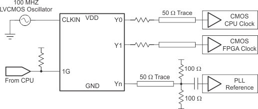
 Figure 7. Example System Configuration
9.2.1 Design Requirements
The CDCVF2310 shown in Figure 7 is configured to fan out a 100-MHz signal from a local LVCMOS oscillator. The CPU is configured to control the output state through 1G.
The configuration example is driving three LVCMOS receivers in a backplane application with the following properties:
- The CPU clock can accept a full swing DC-coupled LVCMOS signal. A series resistor is placed near the CDCVF2310 to closely match the characteristic impedance of the trace to minimize reflections.
- The FPGA clock is similarly DC-coupled with an appropriate series resistor placed near the CDCVF2310.
- The PLL in this example can accept a lower amplitude signal, so a Thevenin's equivalent termination is used. The PLL receiver features internal biasing, so AC-coupling can be used when common-mode voltage is mismatched.
9.2.2 Detailed Design Procedure
Refer to Electrical Characteristics table to determine the appropriate series resistance needed for matching the output impedance of the CDCVF2310 to that of the characteristic impedance of the transmission line.
9.2.3 Application Curves

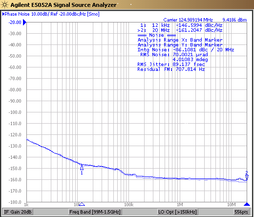
(12 kHz to 20 MHz), Reference Phase Noise 76.9 fs, Output Frequency 125 MHz

(12kHz to 5MHz), Reference Phase Noise 161.5 fs, Frequency 30.72 MHz
The low-additive jitter of the CDCVF2310 can be seen in the previous application plots. The low-noise, 125-MHz input source drives the CDCVF2310, resulting in 45-fs RMS additive jitter when integrated from 12 kHz to 20 MHz for this configuration. The low-noise 30.72-MHz input source drives the CDCVF2310, resulting in 52-fs RMS additive jitter when integrated from 12 kHz to 5 MHz for this configuration.
 Figure 10. CDCVF2310 Configured as Gate Function for Output Clock
The CDCVF2310 can be configured to generate a gated clock using the GN Please refer to Output Enable Glitch Suppression Circuit for required timings.