SLPS261B March 2010 – September 2014 CSD17309Q3
PRODUCTION DATA.
- 1Features
- 2Applications
- 3Description
- 4Revision History
- 5Specifications
- 6Device and Documentation Support
- 7Mechanical, Packaging, and Orderable Information
パッケージ・オプション
デバイスごとのパッケージ図は、PDF版データシートをご参照ください。
メカニカル・データ(パッケージ|ピン)
- DQG|8
サーマルパッド・メカニカル・データ
発注情報
1 Features
- Optimized for 5 V Gate Drive
- Ultra-Low Qg and Qgd
- Low Thermal Resistance
- Avalanche Rated
- Pb Free Terminal Plating
- RoHS Compliant
- Halogen Free
- SON 3.3 mm × 3.3 mm Plastic Package
2 Applications
- Notebook Point of Load
- Point of Load Synchronous Buck in Networking, Telecom, and Computing Systems
3 Description
This 30 V, 4.2 mΩ NexFET™ power MOSFET is designed to minimize losses in power conversion applications and optimized for 5 V gate drive applications.
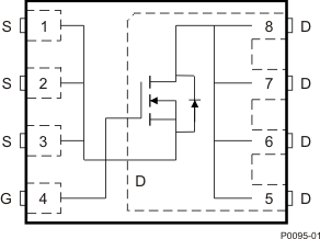
Top View
Product Summary
| TA = 25°C | TYPICAL VALUE | UNIT | ||
|---|---|---|---|---|
| VDS | Drain-to-Source Voltage | 30 | V | |
| Qg | Gate Charge Total (4.5 V) | 7.5 | nC | |
| Qgd | Gate Charge Gate-to-Drain | 1.7 | nC | |
| RDS(on) | Drain-to-Source On-Resistance | VGS = 3 V | 6.3 | mΩ |
| VGS = 4.5 V | 4.9 | |||
| VGS = 8 V | 4.2 | |||
| VGS(th) | Threshold Voltage | 1.2 | V | |
Ordering Information(1)
| Device | Media | Qty | Package | Ship |
|---|---|---|---|---|
| CSD17309Q3 | 13-Inch Reel | 2500 | SON 3.3 × 3.3 mm Plastic Package | Tape and Reel |
| CSD17309Q3T | 7-Inch Reel | 250 |
- For all available packages, see the orderable addendum at the end of the data sheet.
Absolute Maximum Ratings
| TA = 25°C | VALUE | UNIT | |
|---|---|---|---|
| VDS | Drain-to-Source Voltage | 30 | V |
| VGS | Gate-to-Source Voltage | +10 / –8 | V |
| ID | Continuous Drain Current, TC = 25°C | 60 | A |
| Continuous Drain Current(1) | 20 | A | |
| IDM | Pulsed Drain Current, TA = 25°C(2) | 112 | A |
| PD | Power Dissipation(1) | 2.8 | W |
| TJ, Tstg |
Operating Junction and Storage Temperature Range |
–55 to 150 | °C |
| EAS | Avalanche Energy, Single Pulse ID = 57 A, L = 0.1 mH, RG = 25 Ω |
162 | mJ |
- Typical RθJA = 45°C/W when mounted on a 1 inch2 (6.45 cm2), 2 oz. (0.071 mm thick) Cu pad on a
0.06 inch (1.52 mm) thick FR4 PCB. - Pulse duration ≤300 μs, duty cycle ≤2%.
RDS(on) vs VGS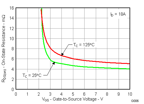 |
Gate Charge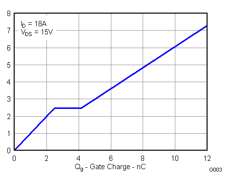 |