SLPS431B June 2013 – December 2014 CSD22202W15
PRODUCTION DATA.
- 1Features
- 2Applications
- 3Description
- 4Revision History
- 5Specifications
- 6Device and Documentation Support
- 7Mechanical, Packaging, and Orderable Information
パッケージ・オプション
デバイスごとのパッケージ図は、PDF版データシートをご参照ください。
メカニカル・データ(パッケージ|ピン)
- YZF|9
サーマルパッド・メカニカル・データ
発注情報
5 Specifications
5.1 Electrical Characteristics
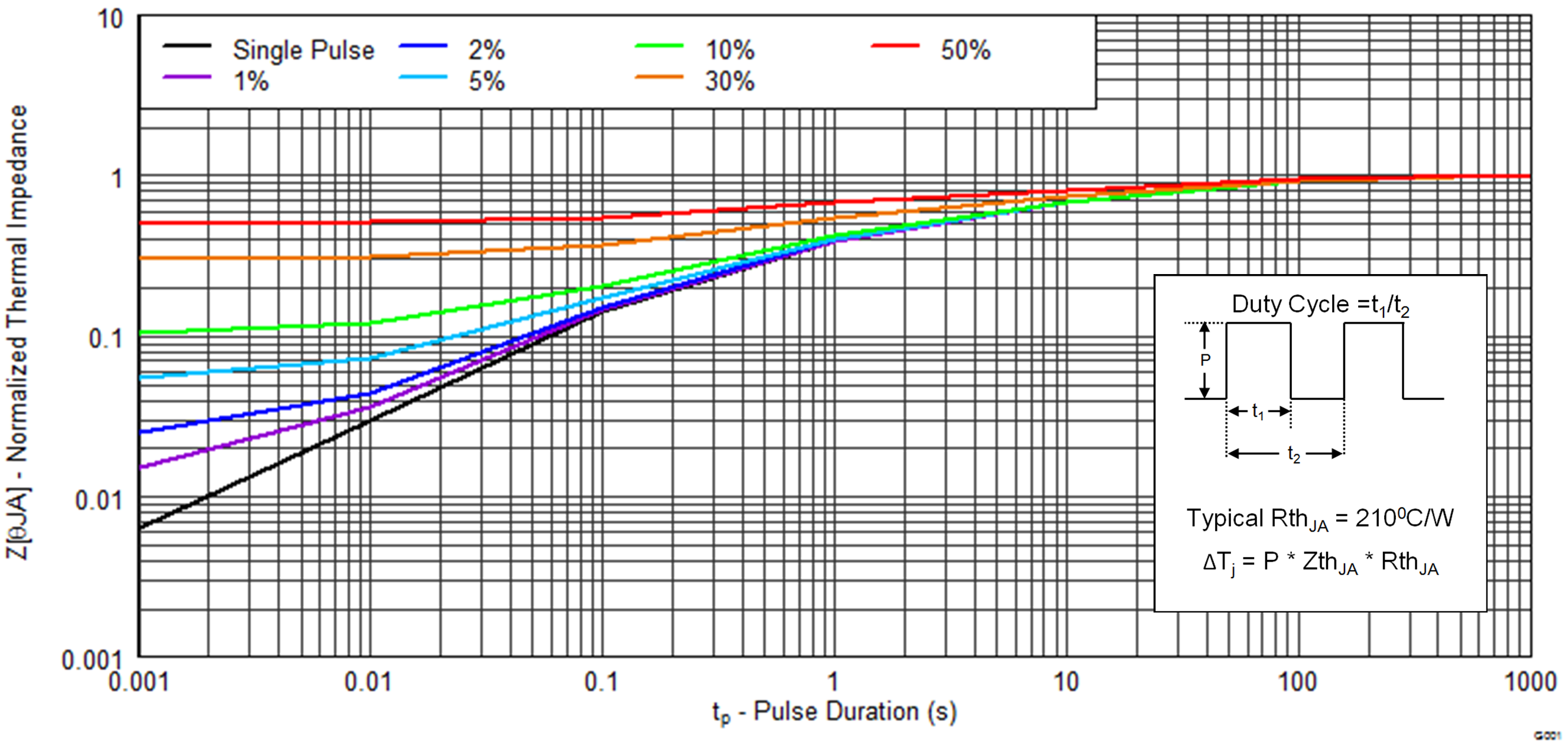
(TA = 25°C unless otherwise stated)5.2 Thermal Information
(TA = 25°C unless otherwise stated)| THERMAL METRIC | TYPICAL VALUES | UNIT | |||
|---|---|---|---|---|---|
| RθJA | Junction-to-Ambient Thermal Resistance(1) | 75 | °C/W | ||
| Junction-to-Ambient Thermal Resistance(2) | 210 | ||||
(1) Device mounted on FR4 material with 1-inch2 (6.45-cm2), 2-oz. (0.071-mm thick) Cu.
(2) Device mounted on FR4 material with minimum Cu mounting area.
 |
Typ RθJA = 75°C/W when mounted on 1inch2 of 2 oz. Cu. |
 |
Typ RθJA = 210°C/W when mounted on minimum pad area of 2 oz. Cu. |
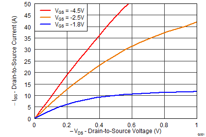
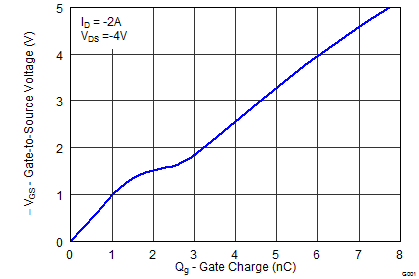
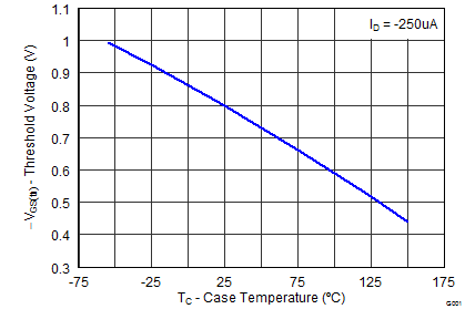
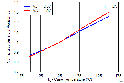
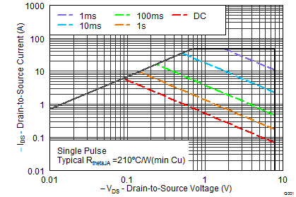
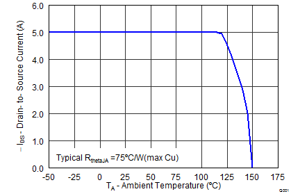
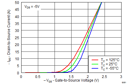
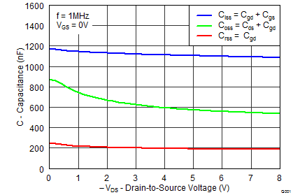
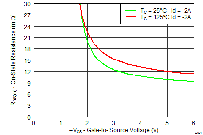
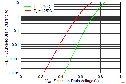
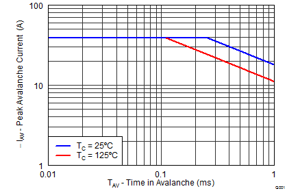
5.3 Typical MOSFET Characteristics
(TA = 25°C unless otherwise stated)