SLPS542 January 2015 CSD97394Q4M
PRODUCTION DATA.
- 1 Features
- 2 Applications
- 3 Description
- 4 Revision History
- 5 Pin Configuration and Functions
- 6 Specifications
- 7 Electrical Characteristics
- 8 Detailed Description
- 9 Application and Implementation
- 10System Example
- 11Layout
- 12Device and Documentation Support
- 13Mechanical, Packaging, and Orderable Information
10 System Example
10.1 Power Loss Curves
MOSFET centric parameters such as RDS(ON) and Qgd are primarily needed by engineers to estimate the loss generated by the devices. In an effort to simplify the design process for engineers, Texas Instruments has provided measured power loss performance curves. Figure 4 plots the power loss of the CSD97394Q4M as a function of load current. This curve is measured by configuring and running the CSD97394Q4M as it would be in the final application (see Figure 15). The measured power loss is the CSD97394Q4M device power loss which consists of both input conversion loss and gate drive loss. Equation 1 is used to generate the power loss curve.
The power loss curve in Figure 4 is measured at the maximum recommended junction temperature of
TJ = 125°C under isothermal test conditions.
10.2 Safe Operating Curves (SOA)
The SOA curves in the CSD97394Q4M datasheet give engineers guidance on the temperature boundaries within an operating system by incorporating the thermal resistance and system power loss. Figure 6 and Figure 8 outline the temperature and airflow conditions required for a given load current. The area under the curve dictates the safe operating area. All the curves are based on measurements made on a PCB design with dimensions of 4.0" (W) x 3.5" (L) x 0.062" (T) and 6 copper layers of 1 oz. copper thickness.
10.3 Normalized Curves
The normalized curves in the CSD97394Q4M data sheet give engineers guidance on the Power Loss and SOA adjustments based on their application specific needs. These curves show how the power loss and SOA boundaries will adjust for a given set of systems conditions. The primary Y-axis is the normalized change in power loss and the secondary Y-axis is the change is system temperature required in order to comply with the SOA curve. The change in power loss is a multiplier for the Power Loss curve and the change in temperature is subtracted from the SOA curve.
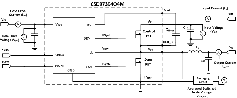 Figure 15. Power Loss Test Circuit
10.3.1 Calculating Power Loss and SOA
The user can estimate product loss and SOA boundaries by arithmetic means (see the Design Example). Though the Power Loss and SOA curves in this datasheet are taken for a specific set of test conditions, the following procedure will outline the steps engineers should take to predict product performance for any set of system conditions.
10.3.1.1 Design Example
Operating Conditions: Output Current (lOUT) = 10 A, Input Voltage (VIN ) = 7 V, Output Voltage (VOUT) = 1.5 V, Switching Frequency (ƒSW) = 800 kHz, Output Inductor (LOUT) = 0.2 µH
10.3.1.2 Calculating Power Loss
- Typical Power Loss at 10 A = 2.1 W (Figure 4)
- Normalized Power Loss for switching frequency ≈ 0.99 (Figure 9)
- Normalized Power Loss for input voltage ≈ 1.10 (Figure 10)
- Normalized Power Loss for output voltage ≈ 0.93 (Figure 11)
- Normalized Power Loss for output inductor ≈ 1.10 (Figure 12)
- Final calculated Power Loss = 2.1 W × 0.99 × 1.10 × 0.93 × 1.10 ≈ 2.3 W
10.3.1.3 Calculating SOA Adjustments
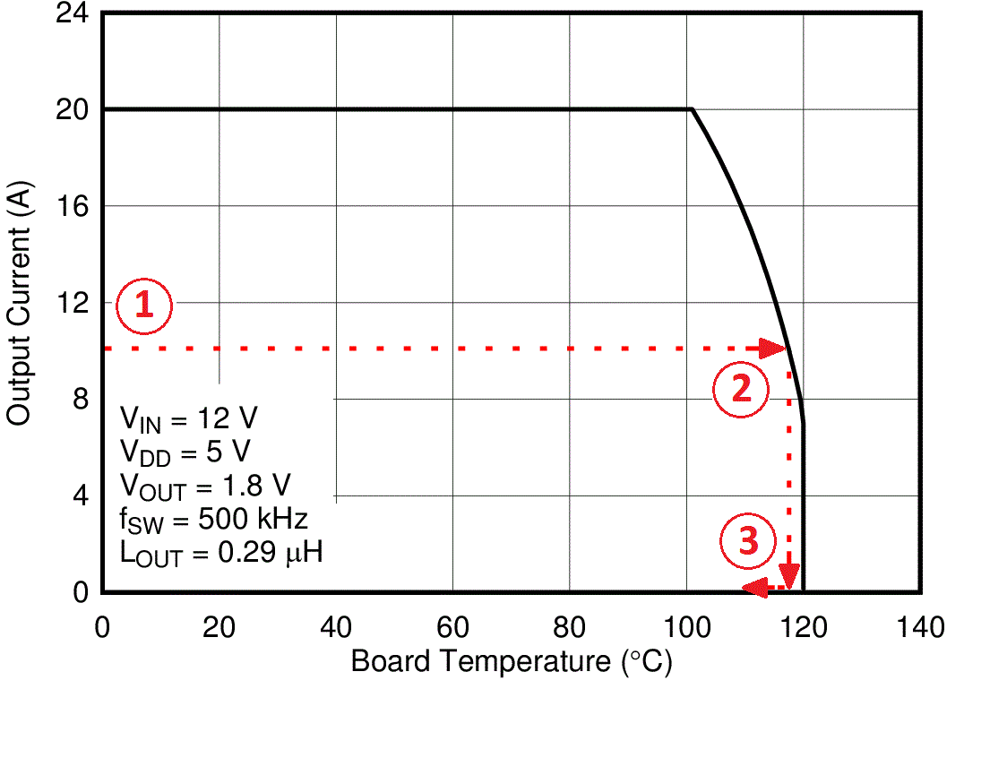 Figure 16. Power Stage CSD97394Q4M SOA
In the design example above, the estimated power loss of the CSD97394Q4M would increase to 2.3 W. In addition, the maximum allowable board and/or ambient temperature would have to decrease by 3.1°C. Figure 16 graphically shows how the SOA curve would be adjusted accordingly.
- Start by drawing a horizontal line from the application current to the SOA curve.
- Draw a vertical line from the SOA curve intercept down to the board/ambient temperature.
- Adjust the SOA board/ambient temperature by subtracting the temperature adjustment value.
In the design example, the SOA temperature adjustment yields a reduction in allowable board/ambient temperature of 3.1°C. In the event the adjustment value is a negative number, subtracting the negative number would yield an increase in allowable board/ambient temperature.