SLPS542 January 2015 CSD97394Q4M
PRODUCTION DATA.
- 1 Features
- 2 Applications
- 3 Description
- 4 Revision History
- 5 Pin Configuration and Functions
- 6 Specifications
- 7 Electrical Characteristics
- 8 Detailed Description
- 9 Application and Implementation
- 10System Example
- 11Layout
- 12Device and Documentation Support
- 13Mechanical, Packaging, and Orderable Information
9 Application and Implementation
NOTE
Information in the following applications sections is not part of the TI component specification, and TI does not warrant its accuracy or completeness. TI’s customers are responsible for determining suitability of components for their purposes. Customers should validate and test their design implementation to confirm system functionality.
9.1 Application Information
The Power Stage CSD97394Q4M is a highly optimized design for synchronous buck applications using NexFET devices with a 5 V gate drive. The Control FET and Sync FET silicon are parametrically tuned to yield the lowest power loss and highest system efficiency. As a result, a rating method is used that is tailored towards a more systems centric environment. The high-performance gate driver IC integrated in the package helps minimize the parasitics and results in extremely fast switching of the power MOSFETs. System level performance curves such as Power Loss, Safe Operating Area and normalized graphs allow engineers to predict the product performance in the actual application.
9.2 Typical Application
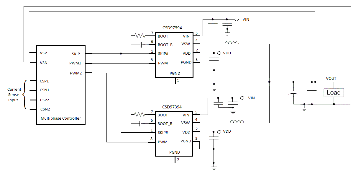 Figure 3. Application Schematic
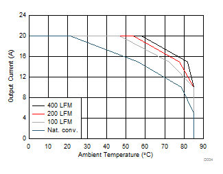
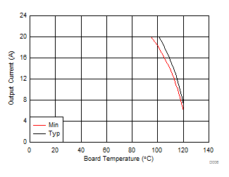
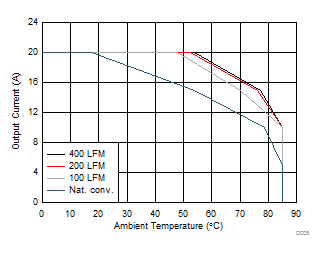
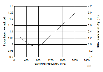
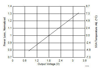
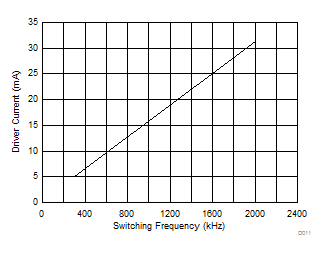
9.2.1 Application Curves
TJ = 125°C, unless stated otherwise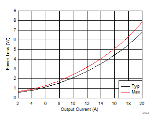
| VIN = 12 V | VDD = 5 V | VOUT = 1.8 V |
| ƒSW = 500 kHz | LOUT = 0.29 µH |
| VIN = 12 V | VDD = 5 V | VOUT = 1.8 V |
| ƒSW = 500 kHz | LOUT = 0.29 µH |
| VIN = 12 V | VDD = 5 V | VOUT = 1.8 V |
| ƒSW = 500 kHz | LOUT = 0.29 µH |
| IOUT = 20 A | VDD = 5 V | VOUT = 1.8 V |
| ƒSW = 500 kHz | LOUT = 0.29 µH |
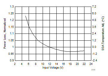
| VIN = 12 V | VDD = 5 V | IOUT = 20 A |
| ƒSW = 500 kHz | VOUT = 1.8 V |
| VIN = 12 V | VDD = 5 V | VOUT = 1.8 V | ||
| IOUT = 20 A | LOUT = 0.29 µH |
| VIN = 12 V | VDD = 5 V | VOUT = 1.8 V |
| ƒSW = 500 kHz | LOUT = 0.29 µH |
| VIN = 12 V | VDD = 5 V | VOUT = 1.8 V |
| ƒSW = 500 kHz | LOUT = 0.29 µH |
| VIN = 12 V | VDD = 5 V | VOUT = 1.8 V |
| IOUT = 20 A | LOUT = 0.29 µH |
| VIN = 12 V | VDD = 5 V | IOUT = 20 A |
| ƒSW = 500 kHz | LOUT = 0.29 µH |
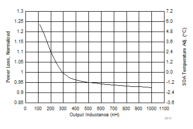
| VIN = 12 V | VDD = 5 V | IOUT = 20 A |
| LOUT = 0.29 µH | VOUT = 1.8 V |
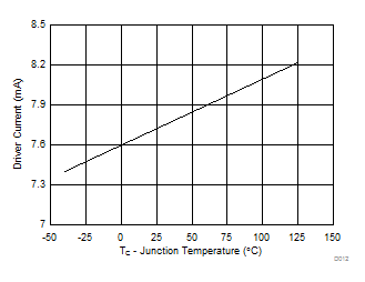
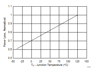
- The Typical CSD97394Q4M System Characteristic curves are based on measurements made on a PCB design with dimensions of 4.0 inches (W) × 3.5 inches (L) × 0.062 inch (T) and 6 copper layers of 1 oz. copper thickness. See the System Example section for detailed explanation.