SLASE16B January 2014 – May 2014 DAC37J82 , DAC38J82
PRODUCTION DATA.
- 1 Features
- 2 Applications
- 3 Description
- 4 Revision History
- 5 Pin Configuration and Functions
-
6 Specifications
- 6.1 Absolute Maximum Ratings
- 6.2 Handling Ratings
- 6.3 Recommended Operating Conditions
- 6.4 Thermal Information
- 6.5 DC Electrical Characteristics
- 6.6 Digital Electrical Characteristics
- 6.7 AC Electrical Characteristics
- 6.8 Timing Requirements
- 6.9 Switching Characteristics
- 6.10 Typical Characteristics
-
7 Detailed Description
- 7.1 Overview
- 7.2 Functional Block Diagram
- 7.3
Feature Description
- 7.3.1 Serdes Input
- 7.3.2 Serdes Rate
- 7.3.3 Serdes PLL
- 7.3.4 Serdes Equalizer
- 7.3.5 JESD204B Descrambler
- 7.3.6 JESD204B Frame Assembly
- 7.3.7 Serial Peripheral Interface (SPI)
- 7.3.8 Multi-Device Synchronization
- 7.3.9 Input Multiplexer
- 7.3.10 FIR Filters
- 7.3.11 Full Complex Mixer
- 7.3.12 Coarse Mixer
- 7.3.13 Dithering
- 7.3.14 Complex Summation
- 7.3.15 Quadrature Modulation Correction (QMC)
- 7.3.16 Group Delay Correction Block
- 7.3.17 Output Multiplexer
- 7.3.18 Power Measurement And Power Amplifier Protection
- 7.3.19 Serdes Test Modes
- 7.3.20 Error Counter
- 7.3.21 Eye Scan
- 7.3.22 JESD204B Pattern Test
- 7.3.23 Temperature Sensor
- 7.3.24 Alarm Monitoring
- 7.3.25 LVPECL Inputs
- 7.3.26 CMOS Digital Inputs
- 7.3.27 Reference Operation
- 7.3.28 Analog Outputs
- 7.3.29 DAC Transfer Function
- 7.4 Device Functional Modes
- 7.5 Register Map
- 8 Applications and Implementation
- 9 Power Supply Recommendations
- 10Layout
- 11Device and Documentation Support
- 12Mechanical, Packaging, and Orderable Information
5 Pin Configuration and Functions
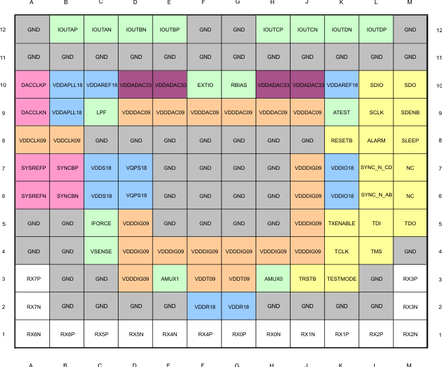
Pin Functions
| PIN | I/O | DESCRIPTION | |
|---|---|---|---|
| NAME | NUMBER | ||
| ALARM | L8 | O | CMOS output for ALARM condition. The ALARM output functionality is defined through the config7 register. Default polarity is active high, but can be changed to active high via config0 alarm_out_pol control bit. If not used it can be left open. |
| AMUX0 | H3 | I/O | Analog test pin for SerDes, Lane 0 to Lane 3. It can be left open if not used. |
| AMUX1 | E3 | I/O | Analog test pin for SerDes, Lane 4 to Lane 7. It can be left open if not used. |
| ATEST | K9 | I/O | Analog test pin for DAC, references and PLL. It can be left open if not used. |
| DACCLKP | A10 | I | Positive LVPECL clock input for DAC core with Vcm = 0.5V. It can be PLL reference clock or external DAC sampling rate clock. If not used, DACCLK is self-biased with 100mV differential at Vcm = 0.5V. |
| DACCLKN | A9 | I | Complementary LVPECL clock input for DAC core. (see the DACCLKP description) |
| EXTIO | F10 | I/O | Used as external reference input when internal reference is disabled through config27 extref_ena = ‘1’. Used as internal reference output when config27 extref_ena = ‘0’ (default). Requires a 0.1 μF decoupling capacitor to analog GND when used as reference output. It can be left open if not used. |
| GND | A12, F12, G12, M12, A11, B11, C11, D11, E11, F11, G11, H11, J11, K11, L11, M11, C8, D8, E8, F8, G8, H8, J8, E7, F7, G7, H7, E6, F6, G6, H6, A5, B5, E5, F5, G5, H5, A4, B4, M4, B3, C3, L3, B2, C2, D2, E2, H2, J2, K2, L2 | I | These pins are ground for all supplies. |
| IFORCE | C5 | I/O | Analog test pin for on chip parametric. It can be left open if not used. |
| IOUTAP | B12 | O | A-Channel DAC current output. Must tied to GND if not used. |
| IOUTAN | C12 | O | A-Channel DAC complementary current output. Must tied to GND if not used. |
| IOUTBP | E12 | O | B-Channel DAC current output. Must tied to GND if not used. |
| IOUTBN | D12 | O | B-Channel DAC complementary current output. Must tied to GND if not used. |
| IOUTCP | H12 | O | C-Channel DAC current output. Must tied to GND if not used. |
| IOUTCN | J12 | O | C-Channel DAC complementary current output. Must tied to GND if not used. |
| IOUTDP | L12 | O | D-Channel DAC current output. Must tied to GND if not used. |
| IOUTDN | K12 | O | D-Channel DAC complementary current output. Must tied to GND if not used. |
| LPF | C9 | I/O | External PLL loop filter connection. It can be left open if not used. |
| RBIAS | G10 | O | Full-scale output current bias. Change the full-scale output current through coarse_dac(3:0). Expected to be 1.92kΩ to GND. |
| RESETB | K8 | I | Active low input for chip RESET, which resets all the programming registers to their default state. Internal pull-up. It can be left open if not used. |
| RX0P | G1 | I | CML SerDes interface lane 0 input, positive, expected to be AC coupled. It can be left open if not used. |
| RX0N | H1 | I | CML SerDes interface lane 0 input, negative, expected to be AC coupled. It can be left open if not used. |
| RX1P | K1 | I | CML SerDes interface lane 1 input, positive, expected to be AC coupled. It can be left open if not used. |
| RX1N | J1 | I | CML SerDes interface lane 1 input, negative, expected to be AC coupled. It can be left open if not used. |
| RX2P | L1 | I | CML SerDes interface lane 2 input, positive, expected to be AC coupled. It can be left open if not used. |
| RX2N | M1 | I | CML SerDes interface lane 2 input, negative, expected to be AC coupled. It can be left open if not used. |
| RX3P | M3 | I | CML SerDes interface lane 3 input, positive, expected to be AC coupled. It can be left open if not used. |
| RX3N | M2 | I | CML SerDes interface lane 3 input, negative, expected to be AC coupled. It can be left open if not used. |
| RX4P | F1 | I | CML SerDes interface lane 4 input, positive, expected to be AC coupled. It can be left open if not used. |
| RX4N | E1 | I | CML SerDes interface lane 4 input, negative, expected to be AC coupled. It can be left open if not used. |
| RX5P | C1 | I | CML SerDes interface lane 5 input, positive, expected to be AC coupled. It can be left open if not used. |
| RX5N | D1 | I | CML SerDes interface lane 5 input, negative, expected to be AC coupled. It can be left open if not used. |
| RX6P | B1 | I | CML SerDes interface lane 6 input, positive, expected to be AC coupled. It can be left open if not used. |
| RX6N | A1 | I | CML SerDes interface lane 6 input, negative, expected to be AC coupled. It can be left open if not used. |
| RX7P | A3 | I | CML SerDes interface lane 7 input, positive, expected to be AC coupled. It can be left open if not used. |
| RX7N | A2 | I | CML SerDes interface lane 7 input, negative, expected to be AC coupled. It can be left open if not used. |
| SYSREFP | A7 | I | LVPECL SYSREF positive input with Vcm = 0.5V. This positive/negative pair is captured with the rising edge of DACCLKP/N. It is used for JESD204B Subclass 1 deterministic latency and multiple DAC synchronization, which can be periodic or pulsed. If not used, it is self-biased with 100mV differential at Vcm = 0.5V. |
| SYSREFN | A6 | I | LVPECL SYSREF negative input with Vcm = 0.5V. (See the SYSREFP description) |
| SCLK | L9 | I | Serial interface clock. Internal pull-down. It can be left open if not used. |
| SDENB | M9 | I | Active low serial data enable, always an input to the DAC37J82/DAC38J82. Internal pull-up. It can be left open if not used. |
| SDIO | L10 | I/O | Serial interface data. Bi-directional in 3-pin mode (default) and 4-pin mode. Internal pull-down. It can be left open if not used. |
| SDO | M10 | O | Uni-directional serial interface data in 4-pin mode. The SDO pin is tri-stated in 3-pin interface mode (default). It can be left open if not used. |
| SLEEP | M8 | I | Active high asynchronous hardware power-down input. Internal pull-down. It can be left open if not used. |
| SYNCBP | B7 | O | Synchronization request to transmitter, LVDS positive output. It can be left open if not used. |
| SYNCBN | B6 | O | Synchronization request to transmitter, LVDS negative output. It can be left open if not used. |
| SYNC_N_AB | L6 | O | Synchronization request to transmitter, CMOS output. Defaults to link 0, but can be programmable for any link. It can be left open if not used. |
| SYNC_N_CD | L7 | O | Synchronization request to transmitter, CMOS output. Defaults to link 1, but can be programmable for any link. It can be left open if not used. |
| TCLK | K4 | I | JTAG test clock. It can be left open if not used. |
| TDI | L5 | I | JTAG test data in. It can be left open if not used. |
| TDO | M5 | O | JTAG test data out. It can be left open if not used. |
| TMS | L4 | I | JTAG test mode select. It can be left open if not used. |
| TRSTB | J3 | I | JTAG test reset. Must be tied to GND to hold the JTAG state machine status reset if the JTAG port is not used. |
| TXENABLE | K5 | I | To enable analog output data transmission, set sif_txenable in register config3 to “1” or pull CMOS TXENABLE pin to high. Transmit enable active high input. Internal pull-down. To disable analog output, set sif_txenable to “0” and pull CMOS TXENABLE pin to low. The DAC output is forced to midscale. It can be left open if not used. |
| TESTMODE | K3 | O | This pin is used for factory testing. Internal pull-down. It can be left open if not used. |
| VDDADAC33 | D10, E10, H10, J10, | I | Analog supply voltage. (3.3V) |
| VDDAPLL18 | B10, B9 | I | PLL analog supply voltage. (1.8V) |
| VDDAREF18 | C10, K10 | I | Analog reference supply voltage (1.8V) |
| VDDCLK09 | A8, B8 | I | Internal clock buffer supply voltage (0.9V). It is recommended to isolate this supply from VDDDIG09. |
| VDDDAC09 | D9, E9, F9, G9, H9, J9 | I | DAC core supply voltage. (0.9V). It is recommended to isolate this supply from VDDDIG09. |
| VDDDIG09 | J7, J6, D5, J5, D4, E4, F4, G4, H4, J4, D3 | I | Digital supply voltage. (0.9V). It is recommended to isolate this supply from VDDCLK09 and VDDDAC09. |
| VDDIO18 | K7, K6 | I | Supply voltage for all digital I/O and CMOS I/O. (1.8V) |
| VDDR18 | F2, G2 | I | Supply voltage for SerDes (1.8V) |
| VDDS18 | C7, C6 | I | Supply voltage for LVDS SYNCBP/N (1.8V) |
| VDDT09 | F3, G3 | I | Supply voltage for SerDes termination (0.9V) |
| VQPS18 | D7, D6 | I | Fuse supply voltage. This supply pin is also used for factory fuse programming. Connect to 1.8V. |
| VSENSE | C4 | I/O | Analog test pin for on chip parametric. It can be left open if not used. |