SGLS387H July 2007 – August 2016 DAC5675A-SP
PRODUCTION DATA.
- 1 Features
- 2 Applications
- 3 Description
- 4 Revision History
- 5 Description (continued)
- 6 Pin Configuration and Functions
-
7 Specifications
- 7.1 Absolute Maximum Ratings
- 7.2 ESD Ratings
- 7.3 Recommended Operating Conditions
- 7.4 Thermal Information
- 7.5 DC Electrical Characteristics (Unchanged After 100 kRad)
- 7.6 AC Electrical Characteristics (Unchanged After 100 kRad)
- 7.7 Digital Specifications (Unchanged After 100 kRad)
- 7.8 Electrical Characteristics
- 7.9 Typical Characteristics
- 8 Detailed Description
- 9 Application and Implementation
- 10Power Supply Recommendations
- 11Layout
- 12Device and Documentation Support
- 13Mechanical, Packaging, and Orderable Information
パッケージ・オプション
デバイスごとのパッケージ図は、PDF版データシートをご参照ください。
メカニカル・データ(パッケージ|ピン)
- HFG|52
サーマルパッド・メカニカル・データ
発注情報
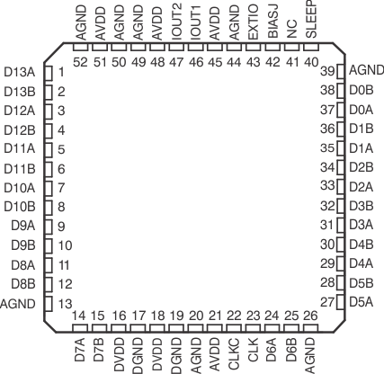
6 Pin Configuration and Functions
HFG Package
52-Pin CQFP
(Top View)

Pin Functions
| PIN | I/O | DESCRIPTION | |
|---|---|---|---|
| NAME | NO. | ||
| AGND | 13, 20, 26, 39, 44, 49, 50, 52 | I | Analog negative supply voltage (ground). Pin 13 is internally connected to the heat slug and lid (lid is also grounded internally). |
| AVDD | 21, 45, 48, 51 | I | Analog positive supply voltage |
| BIASJ | 42 | O | Full-scale output current bias |
| CLK | 23 | I | External clock input |
| CLKC | 22 | I | Complementary external clock |
| D[13:0]A | 1, 3, 5, 7, 9, 11, 14, 24, 27, 29, 31, 33, 35, 37 | I | LVDS positive input, data bits 13–0. D13A is the most significant data bit (MSB). D0A is the least significant data bit (LSB). |
| D[13:0]B | 2, 4, 6, 8, 10, 12, 15, 25, 28, 30, 32, 34, 36, 38 | I | LVDS negative input, data bits 13–0. D13B is the most significant data bit (MSB). D0B is the least significant data bit (LSB). |
| DGND | 17, 19 | I | Digital negative supply voltage (ground) |
| DVDD | 16, 18 | I | Digital positive supply voltage |
| EXTIO | 43 | I/O | Internal reference output or external reference input. Requires a 0.1-μF decoupling capacitor to AGND when used as reference output. |
| IOUT1 | 46 | O | DAC current output. Full-scale when all input bits are set '0'. Connect the reference side of the DAC load resistors to AVDD. |
| IOUT2 | 47 | O | DAC complementary current output. Full-scale when all input bits are '1'. Connect the reference side of the DAC load resistors to AVDD. |
| NC | 41 | Not connected in chip. Can be high or low. | |
| SLEEP | 40 | I | Asynchronous hardware power-down input. Active high. Internal pulldown. |