JAJSE84D June 2017 – August 2018 DAC60508 , DAC70508 , DAC80508
PRODUCTION DATA.
- 1 特長
- 2 アプリケーション
- 3 概要
- 4 改訂履歴
- 5 概要(続き)
- 6 Device Comparison Table
- 7 Pin Configuration and Functions
- 8 Specifications
-
9 Detailed Description
- 9.1 Overview
- 9.2 Functional Block Diagram
- 9.3 Feature Description
- 9.4 Device Functional Modes
- 9.5 Programming
- 9.6
Register Map
- 9.6.1 NOP Register (address = 0x00) [reset = 0x0000]
- 9.6.2 DEVICE ID Register (address = 0x01) [reset = 0x---]
- 9.6.3 SYNC Register (address = 0x2) [reset = 0xFF00]
- 9.6.4 CONFIG Register (address = 0x3) [reset = 0x0000]
- 9.6.5 GAIN Register (address = 0x04) [reset = 0x---]
- 9.6.6 TRIGGER Register (address = 0x05) [reset = 0x0000]
- 9.6.7 BRDCAST Register (address = 0x6) [reset = 0x0000]
- 9.6.8 STATUS Register (address = 0x7) [reset = 0x0000]
- 9.6.9 DACx Register (address = 0x8 to 0xF) [reset = 0x0000 or 0x8000]
- 10Application and Implementation
- 11Power Supply Recommendations
- 12Layout
- 13デバイスおよびドキュメントのサポート
- 14メカニカル、パッケージ、および注文情報
パッケージ・オプション
メカニカル・データ(パッケージ|ピン)
サーマルパッド・メカニカル・データ
- RTE|16
発注情報
9.5 Programming
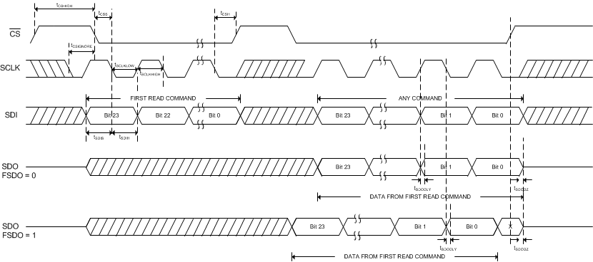
The DACx0508 is controlled through a flexible serial interface that is compatible with SPI type interfaces used on many microcontrollers and DSP controllers. Table 7 shows the SPI timing requirements. Figure 65 and Figure 66 show the SPI write and read timing diagrams, respectively.
Table 7. Programming Timing Requirements(1)
| VIO = 1.7 V to 2.7 V | VIO = 2.7 V to 5.5 V | UNIT | ||||||
|---|---|---|---|---|---|---|---|---|
| MIN | NOM | MAX | MIN | NOM | MAX | |||
| SERIAL INTERFACE – WRITE OPERATION | ||||||||
| fSCLK | SCLK frequency | 50 | 50 | MHz | ||||
| tSCLKHIGH | SCLK high time | 9 | 9 | ns | ||||
| tSCLKLOW | SCLK low time | 9 | 9 | ns | ||||
| tSDIS | SDI setup | 5 | 5 | ns | ||||
| tSDIH | SDI hold | 10 | 10 | ns | ||||
| tCSS | CS to SCLK falling edge setup | 13 | 13 | ns | ||||
| tCSH | SCLK falling edge to CS rising edge | 10 | 10 | ns | ||||
| tCSHIGH | CS high time | 15 | 15 | ns | ||||
| tCSIGNORE | SCLK falling edge to CS ignore | 7 | 7 | ns | ||||
| SERIAL INTERFACE – READ AND DAISY CHAIN OPERATION, FSDO = 0 | ||||||||
| fSCLK | SCLK frequency | 12 | 18 | MHz | ||||
| tSCLKHIGH | SCLK high time | 35 | 25 | ns | ||||
| tSCLKLOW | SCLK low time | 35 | 25 | ns | ||||
| tSDIS | SDI setup | 5 | 5 | ns | ||||
| tSDIH | SDI hold | 10 | 10 | ns | ||||
| tCSS | CS to SCLK falling edge setup | 32 | 20 | ns | ||||
| tCSH | SCLK falling edge to CS rising edge | 10 | 10 | ns | ||||
| tCSHIGH | CS high time | 15 | 15 | ns | ||||
| tSDODLY | SDO output delay from SCLK rising edge | 3.5 | 33.5 | 3.5 | 23 | ns | ||
| tSDODZ | SDO driven to tri-state | 0 | 30 | 0 | 25 | ns | ||
| tCSIGNORE | SCLK falling edge to CS ignore | 7 | 7 | ns | ||||
| SERIAL INTERFACE – READ AND DAISY CHAIN OPERATION, FSDO = 1 | ||||||||
| fSCLK | SCLK frequency | 20 | 25 | MHz | ||||
| tSCLKHIGH | SCLK high time | 22 | 18 | ns | ||||
| tSCLKLOW | SCLK low time | 22 | 18 | ns | ||||
| tSDIS | SDI setup | 5 | 5 | ns | ||||
| tSDIH | SDI hold | 10 | 10 | ns | ||||
| tCSS | CS to SCLK falling edge setup | 32 | 20 | ns | ||||
| tCSH | SCLK falling edge to CS rising edge | 10 | 10 | ns | ||||
| tCSHIGH | CS high time | 15 | 15 | ns | ||||
| tSDODLY | SDO output delay from SCLK falling edge | 3.5 | 45 | 3.5 | 32 | ns | ||
| tSDODZ | SDO driven to tri-state | 0 | 30 | 0 | 25 | ns | ||
| tCSIGNORE | SCLK falling edge to CS ignore | 7 | 7 | ns | ||||
| DIGITAL LOGIC | ||||||||
| tRSTDLYPOR | POR reset delay | 170 | 250 | 170 | 250 | µs | ||
| tDACWAIT | Sequential DAC output updates | 1 | 1 | µs | ||||
| tCLR | CLR pulse | 20 | 20 | ns | ||||
| tCLRD | CLR delay(2) | 100 | 100 | ns | ||||
(1) All input signals are specified with tR = tF = 1 ns/V (10% to 90% of VIO), timed from a voltage level of (VIL + VIH)/2, VDD = 2.7 V to 5.5 V, VIO = 1.7 V to 5.5 V, VREFIN = 1.25 V to 5.5 V, SDO loaded with 20 pF, TA = -40°C to +125°C
(2) Specified from a logic-low on CLR pin to when the DAC output starts to change. In the special case when the DAC output is at GND or VDD, the CLR delay may be as long as 1 µs
 Figure 65. Serial Interface Write Timing Diagram
  Figure 66. Serial Interface Read Timing Diagram