JAJSRE8A October   2015  – September 2023 DLPA3000

PRODUCTION DATA  

  1.   1
  2. 特長
  3. アプリケーション
  4. 概要
  5. Revision History
  6. 概要 (続き)
  7. Pin Configuration and Functions
  8. Specifications
    1. 7.1 Absolute Maximum Ratings
    2. 7.2 ESD Ratings
    3. 7.3 Recommended Operating Conditions
    4. 7.4 Thermal Information
    5. 7.5 Electrical Characteristics
    6. 7.6 SPI Timing Parameters
  9. Detailed Description
    1. 8.1 Overview
    2. 8.2 機能ブロック図
    3. 8.3 Feature Description
      1. 8.3.1 Supply and Monitoring
        1. 8.3.1.1 Supply
        2. 8.3.1.2 Monitoring
          1. 8.3.1.2.1 Block Faults
          2. 8.3.1.2.2 Low Battery and UVLO
          3. 8.3.1.2.3 Auto LED Turn Off Functionality
          4. 8.3.1.2.4 Thermal Protection
      2. 8.3.2 Illumination
        1. 8.3.2.1 Programmable Gain Block
        2. 8.3.2.2 LDO Illum
        3. 8.3.2.3 Illumination Driver A
        4. 8.3.2.4 RGB Strobe Decoder
          1. 8.3.2.4.1 Break Before Make (BBM)
          2. 8.3.2.4.2 Openloop Voltage
          3. 8.3.2.4.3 Transient Current Limit
        5. 8.3.2.5 Illumination Monitoring
          1. 8.3.2.5.1 Power Good
          2. 8.3.2.5.2 Ratio Metric Overvoltage Protection
        6. 8.3.2.6 Load Current and Supply Voltage
        7. 8.3.2.7 Illumination Driver Plus Power FETS Efficiency
      3. 8.3.3 DMD Supplies
        1. 8.3.3.1 LDO DMD
        2. 8.3.3.2 DMD HV Regulator
          1. 8.3.3.2.1 Power-Up and Power-Down Timing
        3. 8.3.3.3 DMD/DLPC Buck Converters
        4. 8.3.3.4 DMD Monitoring
          1. 8.3.3.4.1 Power Good
          2. 8.3.3.4.2 Overvoltage Fault
      4. 8.3.4 Buck Converters
        1. 8.3.4.1 LDO Bucks
        2. 8.3.4.2 General Purpose Buck Converters
        3. 8.3.4.3 Buck Converter Monitoring
          1. 8.3.4.3.1 Power Good
          2. 8.3.4.3.2 Overvoltage Fault
        4. 8.3.4.4 Buck Converter Efficiency
      5. 8.3.5 Auxiliary LDOs
      6. 8.3.6 Measurement System
      7. 8.3.7 Digital Control
        1. 8.3.7.1 SPI
        2. 8.3.7.2 Interrupt
        3. 8.3.7.3 Fast-Shutdown in Case of Fault
    4. 8.4 Device Functional Modes
    5. 8.5 Register Maps
  10. Application and Implementation
    1. 9.1 Application Information
    2. 9.2 Typical Applications
      1. 9.2.1 Typical Application Setup Using DLPA3000
        1. 9.2.1.1 Design Requirements
        2. 9.2.1.2 Detailed Design Procedure
        3. 9.2.1.3 Application Curve
      2. 9.2.2 Typical Application with DLPA3000 Internal Block Diagram
  11. 10Power Supply Recommendations
  12. 11Layout
    1. 11.1 Layout Guidelines
    2. 11.2 Layout Example
    3. 11.3 SPI Connections
    4. 11.4 RLIM Routing
    5. 11.5 LED Connection
    6. 11.6 Thermal Considerations
  13. 12Device and Documentation Support
    1. 12.1 サード・パーティ製品に関する免責事項
    2. 12.2 Device Support
      1. 12.2.1 Device Nomenclature
    3. 12.3 Related Links
    4. 12.4 ドキュメントの更新通知を受け取る方法
    5. 12.5 サポート・リソース
    6. 12.6 Trademarks
    7. 12.7 サポート・リソース
    8. 12.8 静電気放電に関する注意事項
    9. 12.9 用語集
  14. 13Mechanical, Packaging, and Orderable Information

パッケージ・オプション

メカニカル・データ(パッケージ|ピン)
サーマルパッド・メカニカル・データ
発注情報

Illumination

The illumination function includes all blocks needed to generate light for the DLP system. To set the current through the LEDs accurately, use a control loop (Figure 8-4). The intended LED current is set through IDAC[9:0]. The Illumination driver controls the LED anode voltage VLED and as a result a current flows through one of the LEDs. The LED current is measured from the voltage across sense resistor RLIM. Based on the difference between the actual and intended current, the loop controls the output of the buck converter (VLED) higher or lower. Which LED conducts the current is controlled by switches P, Q, and R. The Openloop feedback circuitry ensures that the control loop can be closed for cases when there is no path through the LED; for example, when ILED= 0.
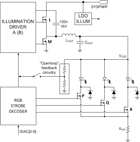
GUID-CD6BF53B-84BF-4F08-9F05-C8521AC4436D-low.gifFigure 8-4 Illumination Control Loop

Within the illumination block, the following blocks can be distinguished:

  • Programmable gain block
  • LDO ILLUM: analog supply voltage for internal illumination blocks
  • Illumination driver A: primary driver using internal FETs
  • Illumination driver B: secondary driver – for future purpose; will not be discussed
  • RGB stobe decoder: driver for external switches to control the on-off rhythm of the LEDs and measures the LED current