JAJSCC7D June   2016  – November 2023 DRV2510-Q1

PRODUCTION DATA  

  1.   1
  2. 特長
  3. アプリケーション
  4. 概要
  5. Revision History
  6. Pin Configuration and Functions
  7. Specifications
    1. 6.1 Absolute Maximum Ratings
    2. 6.2 ESD Ratings
    3. 6.3 Recommended Operating Conditions
    4. 6.4 Thermal Information
    5. 6.5 Electrical Characteristics
    6. 6.6 Timing Requirements
    7. 6.7 Switching Characteristics
    8. 6.8 Typical Characteristics
  8. Detailed Description
    1. 7.1 Overview
    2. 7.2 Functional Block Diagram
    3. 7.3 Feature Description
      1. 7.3.1 Analog Input and Configurable Pre-amplifier
      2. 7.3.2 Pulse-Width Modulator (PWM)
      3. 7.3.3 Designed for low EMI
      4. 7.3.4 Device Protection Systems
        1. 7.3.4.1 Diagnostics
          1. 7.3.4.1.1 Load Diagnostics
        2. 7.3.4.2 Faults During Load Diagnostics
        3. 7.3.4.3 Protection and Monitoring
    4. 7.4 Device Functional Modes
      1. 7.4.1 Operation in Shutdown Mode
      2. 7.4.2 Operation in Standby Mode
      3. 7.4.3 Operation in Active Mode
    5. 7.5 Programming
      1. 7.5.1 General I2C Operation
      2. 7.5.2 Single-Byte and Multiple-Byte Transfers
      3. 7.5.3 Single-Byte Write
      4. 7.5.4 Multiple-Byte Write and Incremental Multiple-Byte Write
      5. 7.5.5 Single-Byte Read
      6. 7.5.6 Multiple-Byte Read
    6. 7.6 Register Map
      1. 7.6.1 Address: 0x01
      2. 7.6.2 Address: 0x02
      3. 7.6.3 Address: 0x03
  9. Application and Implementation
    1. 8.1 Application Information
    2. 8.2 Typical Applications
      1. 8.2.1 Single-Ended Source
        1. 8.2.1.1 Design Requirements
        2. 8.2.1.2 Detailed Design Procedure
          1. 8.2.1.2.1 Optional Components
          2. 8.2.1.2.2 Capacitor Selection
          3. 8.2.1.2.3 Solenoid Selection
          4. 8.2.1.2.4 Output Filter Considerations
        3. 8.2.1.3 Application Curves
        4. 8.2.1.4 Differential Input Diagram
  10. Power Supply Recommendations
  11. 10Layout
    1. 10.1 Layout Guidelines
    2. 10.2 Layout Example
  12. 11Device and Documentation Support
    1. 11.1 Device Support
      1. 11.1.1 サード・パーティ製品に関する免責事項
    2. 11.2 ドキュメントの更新通知を受け取る方法
    3. 11.3 サポート・リソース
    4. 11.4 Trademarks
    5. 11.5 静電気放電に関する注意事項
    6. 11.6 用語集
  13. 12Mechanical, Packaging, and Orderable Information

パッケージ・オプション

メカニカル・データ(パッケージ|ピン)
サーマルパッド・メカニカル・データ
発注情報

Pulse-Width Modulator (PWM)

The DRV2510-Q1 device features BD modulation scheme with high bandwidth, low noise, low distortion, and excellent stability.

The BD modulation scheme allows for smaller ripple currents through the load. Each output switches from 0 V to the supply voltage. With no input, the OUT+ and OUT- pins are in phase with each other so that there is little or no current in the load. For positive differential inputs, the duty cycle of OUT+ is greater than 50% and the duty cycle of OUT- is lower than 50% for a positive differential output voltage. The opposite is true for negative differential inputs. The voltage across the load sits at 0 V throughout most of the switching period, reducing the switching current, which reduces the I2R losses in the load.
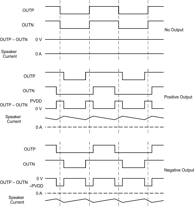
GUID-7DE4D237-23FE-4D54-8097-DBABC42A7A16-low.gif Figure 7-1 BD Mode Modulation