JAJSGK4E March 2013 – January 2023 DRV2667
PRODUCTION DATA
- 1 特長
- 2 アプリケーション
- 3 概要
- 4 Revision History
- 5 Pin Configuration and Functions
- 6 Specifications
-
7 Detailed Description
- 7.1 Overview
- 7.2 Functional Block Diagram
- 7.3
Feature Description
- 7.3.1 Support for Haptic Piezo Actuators
- 7.3.2 Flexible Front End Interface
- 7.3.3 Ramp Down Behavior
- 7.3.4 Low Latency Startup
- 7.3.5 Low Power Standby Mode
- 7.3.6 Device Reset
- 7.3.7 Amplifier Gain
- 7.3.8 Adjustable Boost Voltage
- 7.3.9 Adjustable Current Limit
- 7.3.10 Internal Charge Pump
- 7.3.11 Device Protection
- 7.4 Device Functional Modes
- 7.5 Programming
- 7.6 Register Map
- 8 Application and Implementation
- 9 Power Supply Recommendations
- 10Layout
- 11Device and Documentation Support
- 12Mechanical, Packaging, and Orderable Information
パッケージ・オプション
メカニカル・データ(パッケージ|ピン)
- RGP|20
サーマルパッド・メカニカル・データ
- RGP|20
発注情報
8.1 Application Information
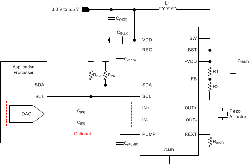
The typical application for a haptic driver is in a touch-enabled system that already has an application processor that makes the decision on when to execute haptic effects.
The DRV2667 device is configured and can be used fully with I2C communication to stream or launch haptic effects. Additionally, the system designer may decide to use the analog input to stream the desired haptic effects.
 Figure 8-1 Typical Application Configuration
Table 8-1 Recommended External Components
| COMPONENT | DESCRIPTION | SPECIFICATION | TYPICAL VALUE |
|---|---|---|---|
| C(VDD) | Input capacitor | Capacitance | 1 µF |
| C(REG) | Regulator capacitor | Capacitance | 0.1 µF |
| C(BST) | Boost capacitor | Capacitance | 0.1 µF |
| CBULK | Bulk capacitor | Capacitance | 10 µF |
| C(PUMP) | Internal charge pump capacitor | Capacitance | 0.1 µF |
| C(IN) | AC coupling capacitor (optional) | Capacitance | 1 µF |
| R1 | Boost feedback resistor (see GUID-97ACC67C-FD5D-46E4-B89F-6BEC952BCD5A.html#GUID-97ACC67C-FD5D-46E4-B89F-6BEC952BCD5A) | Resistance | 768 kΩ |
| R2 | Boost feedback resistor (see GUID-97ACC67C-FD5D-46E4-B89F-6BEC952BCD5A.html#GUID-97ACC67C-FD5D-46E4-B89F-6BEC952BCD5A) | Resistance | 9.76 kΩ |
| R2 | Current limit resistor (see GUID-46CF7CCE-39B0-4967-8A9D-A0D5FCCCE911.html#GUID-46CF7CCE-39B0-4967-8A9D-A0D5FCCCE911) | Resistance | 13 kΩ |
| R(PU) | Pullup resistor | Resistance | 2.2 kΩ |
| L1 | Boost inductor | Inductance | 3.3 µH |