JAJSG61B September   2018  – April 2019 DRV5015-Q1

PRODUCTION DATA.  

  1. 特長
  2. アプリケーション
    1.     代表的な回路図
  3. 概要
    1.     磁気応答
  4. 改訂履歴
  5. Pin Configuration and Functions
    1.     Pin Functions
  6. Specifications
    1. 6.1 Absolute Maximum Ratings
    2. 6.2 ESD Ratings
    3. 6.3 Recommended Operating Conditions
    4. 6.4 Thermal Information
    5. 6.5 Electrical Characteristics
    6. 6.6 Magnetic Characteristics
    7. 6.7 Typical Characteristics
  7. Detailed Description
    1. 7.1 Overview
    2. 7.2 Functional Block Diagram
    3. 7.3 Feature Description
      1. 7.3.1 Magnetic Flux Direction
      2. 7.3.2 Magnetic Response
      3. 7.3.3 Output Driver
      4. 7.3.4 Power-On Time
      5. 7.3.5 Hall Element Location
      6. 7.3.6 Propagation Delay
    4. 7.4 Device Functional Modes
  8. Application and Implementation
    1. 8.1 Application Information
    2. 8.2 Typical Applications
      1. 8.2.1 BLDC Motor Sensors Application
        1. 8.2.1.1 Design Requirements
        2. 8.2.1.2 Detailed Design Procedure
        3. 8.2.1.3 Application Curve
      2. 8.2.2 Incremental Rotary Encoding Application
        1. 8.2.2.1 Design Requirements
        2. 8.2.2.2 Detailed Design Procedure
        3. 8.2.2.3 Application Curve
    3. 8.3 What to Do and What Not to Do
  9. Power Supply Recommendations
  10. 10Layout
    1. 10.1 Layout Guidelines
    2. 10.2 Layout Example
  11. 11デバイスおよびドキュメントのサポート
    1. 11.1 ドキュメントのサポート
      1. 11.1.1 関連資料
    2. 11.2 ドキュメントの更新通知を受け取る方法
    3. 11.3 コミュニティ・リソース
    4. 11.4 商標
    5. 11.5 静電気放電に関する注意事項
    6. 11.6 Glossary
  12. 12メカニカル、パッケージ、および注文情報

パッケージ・オプション

メカニカル・データ(パッケージ|ピン)
サーマルパッド・メカニカル・データ
発注情報

Output Driver

Figure 14 shows the DRV5015-Q1 open-drain output structure. An open-drain output offers flexibility by enabling system designers to interface to wide-range GPIO termination voltages. C1 represents the input capacitance of the GPIO. R1 represents the pullup resistor connected to the termination voltage, VPULL-UP. The maximum allowable value of VPULL_UP is 5.5 V. The value of R1 must be selected after proper considerations among the system speed and the power dissipation through the pullup resistor.
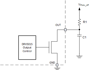
DRV5015-Q1 drv5015-open-drain.gifFigure 14. Open-Drain Output (Simplified)