SLVSCF7B February 2014 – November 2017 DRV8308
PRODUCTION DATA.
- 1 Features
- 2 Applications
- 3 Description
- 4 Revision History
- 5 Pin Configurations and Functions
- 6 Specifications
-
7 Detailed Description
- 7.1 Overview
- 7.2 Functional Block Diagram
- 7.3
Feature Description
- 7.3.1 Hall Comparators
- 7.3.2 FG Amplifier, Comparator, and FG Output
- 7.3.3 Enable, Reset, and Clock Generation
- 7.3.4 Commutation
- 7.3.5 Commutation Logic Block Diagram
- 7.3.6 Commutation Parameters
- 7.3.7 Braking
- 7.3.8 Output Pre-Drivers
- 7.3.9 Current Limit
- 7.3.10 Charge Pump
- 7.3.11 5-V Linear Regulator
- 7.3.12 Power Switch
- 7.3.13 Protection Circuits
- 7.4 Device Functional Modes
- 7.5 Programming
- 7.6 Register Map
- 8 Application and Implementation
- 9 Power Supply Recommendations
- 10Layout
- 11Device and Documentation Support
- 12Mechanical, Packaging, and Orderable Information
パッケージ・オプション
メカニカル・データ(パッケージ|ピン)
- RHA|40
サーマルパッド・メカニカル・データ
- RHA|40
発注情報
1 Features
- Three-Phase Brushless DC Motor Controller
- Digital Closed-Loop Speed Control with Programmable Gain and Filters
- Drives 6 N-Channel MOSFETs With Configurable 10- to 130-mA Gate Drive
- Integrated Commutation from Hall Sensors
- Timing Can Be Advanced/Delayed
- 120° or 180°-Sinusoidal Current Control
- Single Input Controls Motor Speed
- Operating Supply Voltage 8.5 to 32 V
- Flexible Configuration Methods
- Read Internal Non-Volatile Memory
- Read External EEPROM
- Write SPI
- Configurable Motor Current Limiter
- 5-V Regulator for Hall Sensors
- Low-power Standby Mode
- Integrated Overcurrent, Overvoltage, and Overtemperature Protection
2 Applications
- Industrial Pumps, Fans, and Valves
- White Goods
- Power Tools and Lawn Equipment
- Printers
3 Description
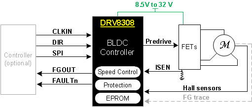
The DRV8308 controls sensored brushless DC motors with advanced features and a simple input interface. As a predriver, it drives the gates of 6 external N-Channel MOSFETs with a configurable current of 10mA to 130mA for optimal switching characteristics.
The 3 motor phases are commutated according to the Hall sensor inputs. Once the motor reaches a consistent speed, the DRV8308 uses just 1 Hall sensor to minimize jitter caused by sensor mismatch. The Hall signal-to-drive timing can be advanced or delayed in 0.1% increments to optimize power efficiency. An optional 180° commutation mode drives sinusoidal current through the motor and minimizes audible noise and torque ripple. Peak motor current can be controlled by sizing a sense resistor.
The DRV8308 achieves closed-loop speed control to spin motors to a precise RPM across a wide range of load torques. The system matches motor speed—generated from an FG trace or the Hall sensors—to the reference frequency on pin CLKIN. The DRV8308 can also drive motors open-loop using a duty cycle command, from either a clock or register setting.
An assortment of protection features bolster system robustness, as the DRV8308 handles and reports overcurrent, overvoltage, undervoltage, and overtemperature.
Device Information(1)
| PART NUMBER | PACKAGE | BODY SIZE (NOM) |
|---|---|---|
| DRV8308 | VQFN (40) | 6.00 mm × 6.00 mm |
- For all available packages, see the orderable addendum at the end of the datasheet.
Simplified Schematic
