SLVSBA5D October 2012 – April 2016 DRV8313
PRODUCTION DATA.
- 1 Features
- 2 Applications
- 3 Description
- 4 Revision History
- 5 Pin Configuration and Functions
- 6 Specifications
- 7 Detailed Description
- 8 Application and Implementation
- 9 Power Supply Recommendations
- 10Layout
- 11Device and Documentation Support
- 12Mechanical, Packaging, and Orderable Information
パッケージ・オプション
メカニカル・データ(パッケージ|ピン)
サーマルパッド・メカニカル・データ
発注情報
10 Layout
10.1 Layout Guidelines
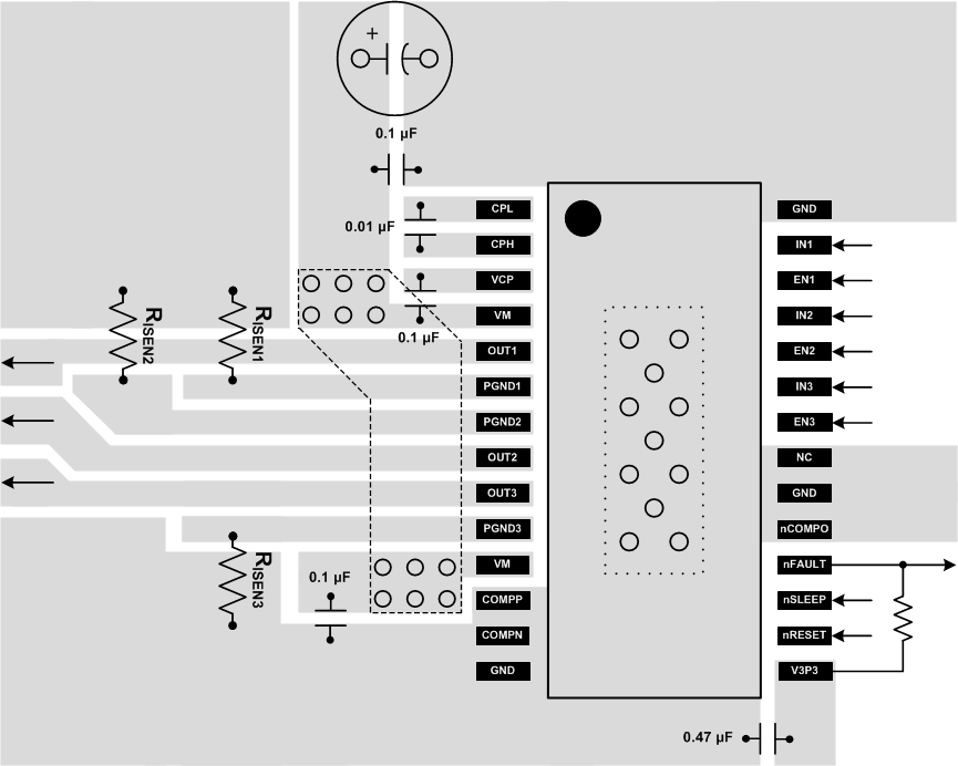
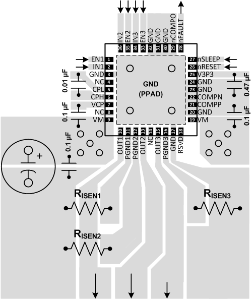
The bulk capacitor should be placed to minimize the distance of the high-current path through the motor driver device. The connecting metal trace widths should be as wide as possible, and numerous vias should be used when connecting PCB layers. These practices minimize inductance and allow the bulk capacitor to deliver high current.
Small-value capacitors should be ceramic, and placed closely to device pins.
The high-current device outputs should use wide metal traces.
The device thermal pad should be soldered to the PCB top-layer ground plane. Multiple vias should be used to connect to a large bottom-layer ground plane. The use of large metal planes and multiple vias helps dissipate the I2 × rDS(on) heat that is generated in the device.
In Figure 19 and Figure 20, the uncommitted comparator is not used. Because this is the case, the COMPP, COMPN, and COMPO pins are tied to GND.
10.2 Layout Example
 Figure 19. Recommended Layout Example For HTSSOP PWP Package
 Figure 20. Recommended Layout Example For QFN RHH Package
10.3 Thermal Considerations
The DRV8313 has thermal shutdown (TSD) as previously described. A die temperature in excess of 150°C (minimally) disables the device until the temperature drops to a safe level.
Any tendency of the device to enter thermal shutdown is an indication of excessive power dissipation, insufficient heatsinking, or too high an ambient temperature.
10.3.1 Heatsinking
The PowerPAD package uses an exposed pad to remove heat from the device. For proper operation, this pad must be thermally connected to copper on the PCB to dissipate heat. On a multi-layer PCB with a ground plane, add a number of vias to connect the thermal pad to the ground plane to accomplish this. On PCBs without internal planes, add copper area on either side of the PCB to dissipate heat. If the copper area is on the opposite side of the PCB from the device, use thermal vias to transfer the heat between the top and bottom layers.
For details about how to design the PCB, see PowerPAD Thermally Enhanced Package (SLMA002) and PowerPAD Made Easy (SLMA004), which are available at www.ti.com.
In general, providing more copper area allows the dissipation of more power.
10.4 Power Dissipation
The power dissipated in the output FET resistance, or rDS(on) dominates power dissipation in the DRV8313. A rough estimate of average power dissipation of each half-H-bridge when running a static load is:

where
- P is the power dissipation of one H-bridge,
- rDS(on) is the resistance of each FET, and
- IOUT is equal to the average current drawn by the load.
At start-up and fault conditions, this current is much higher than normal running current; remember to take these peak currents and their duration into consideration.
The total device dissipation is the power dissipated in each of the three half-H-bridges added together.
The maximum amount of power that the device can dissipate depends on ambient temperature and heatsinking.
Note that rDS(on) increases with temperature, so as the device heats, the power dissipation increases. Take this into consideration when sizing the heatsink.