JAJSCQ3E October 2016 – January 2021 DRV8702-Q1 , DRV8703-Q1
PRODUCTION DATA
- 1 特長
- 2 アプリケーション
- 3 概要
- 4 Revision History
- 5 Pin Configuration and Functions
- 6 Specifications
-
7 Detailed Description
- 7.1 Overview
- 7.2 Functional Block Diagram
- 7.3
Feature Description
- 7.3.1 Bridge Control
- 7.3.2 MODE Pin
- 7.3.3 nFAULT Pin
- 7.3.4 Current Regulation
- 7.3.5 Amplifier Output (SO)
- 7.3.6 PWM Motor Gate Drivers
- 7.3.7 IDRIVE Pin (DRV8702-Q1 Only)
- 7.3.8 Dead Time
- 7.3.9 Propagation Delay
- 7.3.10 Overcurrent VDS Monitor
- 7.3.11 VDS Pin (DRV8702-Q1 Only)
- 7.3.12 Charge Pump
- 7.3.13 Gate Drive Clamp
- 7.3.14
Protection Circuits
- 7.3.14.1 VM Undervoltage Lockout (UVLO2)
- 7.3.14.2 Logic Undervoltage (UVLO1)
- 7.3.14.3 VCP Undervoltage Lockout (CPUV)
- 7.3.14.4 Overcurrent Protection (OCP)
- 7.3.14.5 Gate Driver Fault (GDF)
- 7.3.14.6 Thermal Shutdown (TSD)
- 7.3.14.7 Watchdog Fault (WDFLT, DRV8703-Q1 Only)
- 7.3.14.8 Reverse Supply Protection
- 7.3.15 Hardware Interface
- 7.4 Device Functional Modes
- 7.5 Programming
- 7.6 Register Maps
- 8 Application and Implementation
- 9 Power Supply Recommendations
- 10Layout
- 11Device and Documentation Support
- 12Mechanical, Packaging, and Orderable Information
パッケージ・オプション
デバイスごとのパッケージ図は、PDF版データシートをご参照ください。
メカニカル・データ(パッケージ|ピン)
- RHB|32
サーマルパッド・メカニカル・データ
発注情報
7.3.4 Current Regulation
The maximum current through the motor winding is regulated by a fixed off-time PWM current regulation or current chopping. When an H-bridge is enabled in forward or reverse drive, current rises through the winding at a rate dependent on the DC voltage and inductance of the winding. When the current hits the current chopping threshold, the bridge enters a brake (low-side slow decay) mode until the toff time expires.
Immediately after the current is enabled, the voltage on the SP pin is ignored for a period (t(BLANK)) before enabling the current-sense circuitry.
The PWM chopping current is set by a comparator that compares the voltage across a current-sense resistor connected to the SP pin, multiplied by a factor of AV, with a reference voltage from the VREF pin. The factor AV is the shunt-amplifier gain, which is 19.8 V/V for the DRV8702-Q1 device or configurable to 10, 19.8, 39.4, or 78 V/V for the DRV8703-Q1 device.
Use Equation 1 to calculate the chopping current (ICHOP).
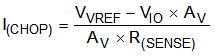
For example, if a 50-mΩ sense resistor and a VREF value of 3.3 V are selected, the full-scale chopping current is 3.28 A. The AV is 19.8 V/V and VIO is assumed to be 50 mV in this example.
For DC motors, current regulation is used to limit the start-up and stall current of the motor. If the current regulation feature is not needed, it can be disabled by tying the VREF pin directly to the AVDD pin. If the independent PWM control-interface mode (MODE pin is 1) is selected for operation, the device does not perform PWM current regulation or current chopping.