SLVSC40H June 2013 – May 2020 DRV8711
PRODUCTION DATA.
- 1 Features
- 2 Applications
- 3 Description
- 4 Revision History
- 5 Pin Configuration and Functions
- 6 Specifications
-
7 Detailed Description
- 7.1 Overview
- 7.2 Functional Block Diagram
- 7.3 Feature Description
- 7.4 Device Functional Modes
- 7.5 Programming
- 7.6
Register Maps
- 7.6.1 Control Registers
- 7.6.2 CTRL Register (Address = 0x00)
- 7.6.3 TORQUE Register (Address = 0x01)
- 7.6.4 OFF Register (Address = 0x02)
- 7.6.5 BLANK Register (Address = 0x03)
- 7.6.6 DECAY Register (Address = 0x04)
- 7.6.7 STALL Register (Address = 0x05)
- 7.6.8 DRIVE Register (Address = 0x06)
- 7.6.9 STATUS Register (Address = 0x07)
- 8 Application and Implementation
- 9 Power Supply Recommendations
- 10Layout
- 11Device and Documentation Support
- 12Mechanical, Packaging, and Orderable Information
パッケージ・オプション
メカニカル・データ(パッケージ|ピン)
- DCP|38
サーマルパッド・メカニカル・データ
- DCP|38
発注情報
7.3.4 Current Regulation
The current through the motor windings is regulated by an adjustable fixed-off-time PWM current regulation circuit. When an H-bridge is enabled, current rises through the winding at a rate dependent on the DC voltage and inductance of the winding and the magnitude of the back EMF present. Once the current hits the current chopping threshold, the bridge disables the current for a fixed period of time, which is programmable between 500 nS and 128 µS by writing to the TOFF bits in the OFF register. After the off time expires, the bridge is re-enabled, starting another PWM cycle.
In stepping motors, current regulation is used to vary the current in the two windings in a sinusoidal fashion to provide smooth motion.
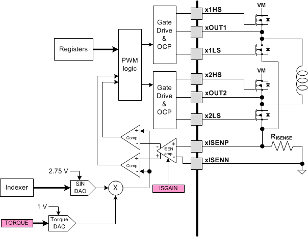
The PWM chopping current is set by a comparator which compares the voltage across a current sense resistor connected to the xISENx pins, multiplied by the gain of the current sense amplifier, with a reference voltage. The current sense amplifier is programmable in the CTRL register.
 Figure 8. PWM Chopping Current
 To generate the reference voltage for the current chopping comparator, the output of a sine lookup table is multiplied by the value of the bits in the TORQUE register. This result is applied to a sine-weighted DAC, whose full-scale output voltage is 2.75 V.
Therefore, the full-scale (100%) chopping current is calculated as follows:

where
- TORQUE is the setting of the TORQUE bits
- ISGAIN is the programmed gain of the ISENSE amplifiers (5, 10, 20, or 40)
Example:
If a 0.1-Ω sense resistor is used, ISGAIN is set to 0 (gain of 5), and TORQUE is set to 255, the full-scale (100%) chopping current will be (2.75 V * 255) / (256 * 5 * 0.1 Ω) = 5.5 A.