SLVSAW5C July 2011 – November 2015 DRV8803
PRODUCTION DATA.
- 1 Features
- 2 Applications
- 3 Description
- 4 Revision History
- 5 Pin Configuration and Functions
- 6 Specification
- 7 Detailed Description
- 8 Application and Implementation
- 9 Power Supply Recommendations
- 10Layout
- 11Device and Documentation Support
- 12Mechanical, Packaging, and Orderable Information
パッケージ・オプション
メカニカル・データ(パッケージ|ピン)
サーマルパッド・メカニカル・データ
- PWP|16
発注情報
7 Detailed Description
7.1 Overview
The DRV8803 device is an integrated 4-channel low side driver solution for any low side switch application. The integrated overcurrent protection limits the motor current to a fixed maximum. Four logic inputs control the low-side driver outputs which consist of four N-channel MOSFETs that have a typical RDS(on) of 500 mΩ. A single power input VM serves as device power and is internally regulated to power the internal low side gate drive. Motor speed can be controlled with pulse-width modulation at frequencies from 0 kHz to 100 kHz. The device outputs can be disabled by bringing nENBL pin high. The thermal shutdown protection enables the device to automatically shut down if the die temperature exceeds a TTSD limit. UVLO protection will disable all circuitry in the device if VM drops below the undervoltage lockout threshold.
7.2 Functional Block Diagram

7.3 Feature Description
7.3.1 Output Drivers
The DRV8803 device contains four protected low-side drivers. Each output has an integrated clamp diode connected to a common pin, VCLAMP.
VCLAMP can be connected to the main power supply voltage, VM. VCLAMP can also be connected to a Zener or TVS diode to VM, allowing the switch voltage to exceed the main supply voltage VM. This connection can be beneficial when driving loads that require very fast current decay, such as unipolar stepper motors.
In all cases, the voltage on the outputs must not be allowed to exceed the maximum output voltage specification.
7.3.2 Protection Circuits
The DRV8803 device is fully protected against undervoltage, overcurrent and overtemperature events.
7.3.2.1 Overcurrent Protection (OCP)
An analog current limit circuit on each FET limits the current through the FET by removing the gate drive. If this analog current limit persists for longer than the tOCP deglitch time (approximately 3.5 µs), the driver will be disabled and the nFAULT pin will be driven low. The driver will remain disabled for the tRETRY retry time (approximately 1.2 ms), then the fault will be automatically cleared. The fault will be cleared immediately if either RESET pin is activated or VM is removed and reapplied.
7.3.2.2 Thermal Shutdown (TSD)
If the die temperature exceeds safe limits, all output FETs will be disabled and the nFAULT pin will be driven low. Once the die temperature has fallen to a safe level, operation will automatically resume.
7.3.2.3 Undervoltage Lockout (UVLO)
If at any time the voltage on the VM pin falls below the undervoltage lockout threshold voltage, all circuitry in the device will be disabled, and internal logic will be reset. Operation will resume when VM rises above the UVLO threshold.
7.4 Device Functional Modes
7.4.1 Parallel Interface Operation
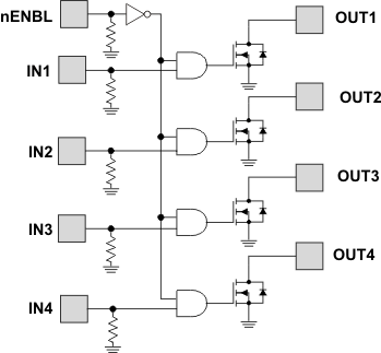
The DRV8803 device is controlled with a simple parallel interface. Logically, the interface is shown in Figure 6.
 Figure 6. Parallel Interface Operation
7.4.2 nENBL and RESET Operation
The nENBL pin enables or disables the output drivers. nENBL must be low to enable the outputs. Note that nENBL has an internal pulldown.
The RESET pin, when driven active high, resets internal logic. All inputs are ignored while RESET is active. Note that RESET has an internal pulldown. An internal power-up reset is also provided, so it is not required to drive RESET at power up.