SLVS857B December 2009 – January 2015 DRV8808
PRODUCTION DATA.
- 1 Features
- 2 Applications
- 3 Description
- 4 Revision History
- 5 Pin Configuration and Functions
- 6 Specifications
-
7 Detailed Description
- 7.1 Overview
- 7.2 Functional Block Diagram
- 7.3
Feature Description
- 7.3.1
Setup Mode, Extended Setup Mode, Power-Down Mode
- 7.3.1.1 Operation Setup Register Bit Assignment
- 7.3.1.2 Operation Extended Setup Register Bit Assignment
- 7.3.1.3 Deep Sleep Mode
- 7.3.1.4 DC Motor Drive
- 7.3.1.5 Short/Open for Motor Outputs
- 7.3.1.6 Charge Pump
- 7.3.1.7 DC-DC Converters
- 7.3.1.8 nReset: Input for System Reset
- 7.3.1.9 VM Start-up/Power-Down and Glitch Condition
- 7.3.2 Blanking Time Insertion Timing for DC Motor Driving
- 7.3.3 Function Table in nORT, Power Down, VM Conditions
- 7.3.1
Setup Mode, Extended Setup Mode, Power-Down Mode
- 7.4 Device Functional Modes
- 7.5 Programming
- 8 Application and Implementation
- 9 Power Supply Recommendations
- 10Layout
- 11Device and Documentation Support
- 12Mechanical, Packaging, and Orderable Information
パッケージ・オプション
メカニカル・データ(パッケージ|ピン)
- DCA|48
サーマルパッド・メカニカル・データ
- DCA|48
発注情報
6 Specifications
6.1 Absolute Maximum Ratings(1)
over operating free-air temperature range (unless otherwise noted)| MIN | MAX | UNIT | ||
|---|---|---|---|---|
| VM | Supply voltage | 40 | V | |
| Logic input voltage, serial I/F, A_CONT, nReset, and so forth (2) | –0.3 | 5.5 | V | |
| TH_OUT, nORT, LOGIC_OUT, CSELECT | –0.3 | 3.6 | V | |
| nWAKEUP | –0.3 | 8 | V | |
| Continuous total power dissipation (in case θJA = 20°C/W) | 4 | W | ||
| Continuous motor-drive output current for each H-bridge (100 ms) | 2.5 | A | ||
| Continuous DC-DC converter output current(3) | 1.35 | A | ||
| TJ | Operating junction temperature (1 hour) | 190 | °C | |
| Lead temperature 1.6 mm (1/16 in) from case for 10 s | 260 | °C | ||
| Tstg | Storage temperature | –65 | 150 | °C |
(1) Stresses beyond those listed under Absolute Maximum Ratings may cause permanent damage to the device. These are stress ratings only and functional operation of the device at these or any other conditions beyond those indicated under Recommended Operating Conditions is not implied. Exposure to absolute-maximum-rated conditions for extended periods may affect device reliability.
(2) The negative spike less than –5 V and narrower than 50-ns width should not cause any problem.
(3) May shut down due to regulator OCP.
6.2 ESD Ratings
| VALUE | UNIT | |||
|---|---|---|---|---|
| V(ESD) | Electrostatic discharge | Human-body model (HBM), per ANSI/ESDA/JEDEC JS-001(1) | ±2000 | V |
| Charged-device model (CDM), per JEDEC specification JESD22-C101(2) | ±500 | |||
(1) JEDEC document JEP155 states that 500-V HBM allows safe manufacturing with a standard ESD control process.
(2) JEDEC document JEP157 states that 250-V CDM allows safe manufacturing with a standard ESD control process.
6.3 Recommended Operating Conditions
| MIN | NOM | MAX | UNIT | |
|---|---|---|---|---|
| Supply voltage range, VM for motor control | 18 | 27 | 38 | V |
| Supply voltage range for DC-DC converter (VM) | 7 | 27 | 38 | V |
| Operating ambient temperature range | –10 | 85 | °C | |
| Operating junction temperature range | 0 | 135 | °C |
6.4 Thermal Information
| THERMAL METRIC(1) | DRV8808 | UNIT | |
|---|---|---|---|
| HTSSOP (DCA) | |||
| 48 PINS | |||
| RθJA | Junction-to-ambient thermal resistance | 28.1 | °C/W |
| RθJC(top) | Junction-to-case (top) thermal resistance | 15.6 | |
| RθJB | Junction-to-board thermal resistance | 10.2 | |
| ψJT | Junction-to-top characterization parameter | 0.3 | |
| ψJB | Junction-to-board characterization parameter | 10.1 | |
| RθJC(bot) | Junction-to-case (bottom) thermal resistance | 0.9 | |
(1) For more information about traditional and new thermal metrics, see the IC Package Thermal Metrics application report, SPRA953.
6.5 Electrical Characteristics
TJ = 0°C to 135°C, VM = 7 V to 38 V (unless otherwise noted)| PARAMETER | TEST CONDITIONS | MIN | TYP | MAX | UNIT | ||
|---|---|---|---|---|---|---|---|
| SUPPLY (SLEEP) CURRENT | |||||||
| ISLEEP1 | Supply (sleep) current 1 | nSLEEP = L, | DC-DC all off | 3 | 5.5 | mA | |
| ISLEEP2 | Supply (sleep) current 2 | nSLEEP = L, Regulators enabled |
VM = 8 V, No load |
6 | 8 | mA | |
| ISLEEP3 | Supply (sleep) current 3 | nSLEEP = L, Regulators enabled |
VM = 38 V, No load |
6 | 8 | mA | |
| IDEEP_SL | Supply (deep sleep) current(1) | VM = 38 V | 0.7 | 1 | mA | ||
| DIGITAL INTERFACE CIRCUIT | |||||||
| VIH | Digital high-level input voltage | Digital inputs | 2 | 3.6 | V | ||
| IIH | Digital high-level input current | Digital inputs | 100 | μA | |||
| VIL | Digital low-level input voltage | Digital inputs | 0.8 | V | |||
| IIL | Digital low-level input current | Digital inputs | 100 | μA | |||
| Vhys | Digital input hysteresis | Digital inputs | 0.45 | V | |||
| Tdeg_nReset | nReset input deglitch time | 2.5 | 7.5 | μs | |||
| Tfilt_ACONT | A_CONT filter time(2) | 30 | 70 | μs | |||
| CHARGE-PUMP VCP (CP = 0.1 μF to 0.47 μF, Cblk = 0.01 μF ±20%) | |||||||
| VO(CP) | Output voltage | ILOAD = 0 mA, | VM > 15 V | VM + 10 | VM + 13 | V | |
| f(CP) | Switching frequency | 1.6 | MHz | ||||
| tstart | Start-up time | CStorage = 0.1 μF, | VM ≥ 15 V | 0.5 | 2 | ms | |
| V3P3 OUTPUT | |||||||
| V3p3 | Output voltage(3) | 3 | 3.3 | 3.6 | V | ||
| Cbypass | Output capacitor | 0.08 | 0.1 | 10 | μF | ||
| INTERNAL CLOCK OSCI | |||||||
| fOSCi | System clock rrequency | 5.76 | 6.4 | 7.04 | MHz | ||
| CSELECT FOR DC-DC STARTUP SELECTION | |||||||
| VCS0 | DC-DC all off | 0 | 0.3 | V | |||
| VCS1 | Turn ON ODB | Pull down by external 200-kΩ resistor | 1.3 | 2 | V | ||
| VCS2 | Turn ON ODB then ODC | As pin open | 3 | 3.6 | V | ||
| VLDO REGULATOR(4)(5)(6) | |||||||
| VLDOIN | LDO input voltage | 3 | 3.6 | V | |||
| VLDOFB | Feedback voltage | 1 | V | ||||
| VLDOOUT | Output voltage range | 1 V ≤ VLDOOUT ≤ 1.8 V | ±5% | ||||
| 1.8 V ≤ VLDOOUT ≤ 2.5 V | ±3% | ||||||
| IOUT | Load capability | 500 | mA | ||||
| IOCP | OCP current | 725 | 1100 | mA | |||
| tIdeg | OCP deglitch | 3 | 8 | 13 | μs | ||
| Vovp | Overvoltage protection | % to nominal Voutx detected at VFB (VFB increasing) |
25% | 30% | 35% | ||
| Vuvp | Undervoltage protection | % to nominal Voutx detected at VFB (VFB decreasing) |
–25% | –30% | –35% | ||
| tVdeg | UVP/OVP deglitch time | 3 | 8 | 13 | μs | ||
| CL1 | Load bypass configuration 1 | Electrolytic load capacitance | 27 | 120 | μF | ||
| CESR1 | ESR of load capacitance | 0.05 | 2 | Ω | |||
| CC1 | Ceramic load capacitance | 0 | 0.4 | μF | |||
| CL2 | Load bypass configuration 2 | Electrolytic load capacitance | 80 | 100 | 120 | μF | |
| CESR2 | ESR of load capacitance | 0.05 | 0.2 | Ω | |||
| CC2 | Ceramic load capacitance | 0 | 3 | μF | |||
| THREE DC-DC CONVERTER | |||||||
| VM OPE_X | Operating supply voltage range ratio to VOUT | IO < 0.6 A | Vth VM- < VM < 7 V | 0.8 x VM | V | ||
| 20 V < VM < 38 V | 0.9 x VM | ||||||
| ODx | Regulator output voltage | 20 V < VM < 40 V | 0℃ < TJ < 125℃ | -3% | VO | 3% | |
| 125℃ < TJ < 135℃ | -4% | VO | 4% | ||||
| 6.5 V < VM < 20 V | -5% | VO | 5% | ||||
| VM = 7 V, VO = 5.5 V | -5% | VO | 5% | ||||
| VM = 7 V, VO = 1 V | 0℃ < TJ < 125℃ | -3% | VO | 3% | |||
| 125℃ < TJ < 135℃ | -4% | VO | 4% | ||||
| VthVM- < VM < 6.5 V , VO ≤ 3.3 V | -5% | VO | 5% | ||||
| FBx | FBx pin voltage | 1 | V | ||||
| IO ODx | Output current (DC) | VM > 15 V | 1.35 | A | |||
| IO ODx2 | Output current (DC) at low VM | VM = 7 V, VO = 5.5 V | 0.6 | A | |||
| IO ODx3 | Output current (DC) at low VM | VM = 7 V, VO = 3.3 V | 1.2 | A | |||
| RDSON(7) | FET on-resistance at 0.8 A for OD_x VM > 15 V | TJ = 70 °C | 0.85 | 1.05 | Ω | ||
| TJ = 135 °C | 1 | 1.2 | |||||
| L | Inductor | VOUT = 1.0 V | 150 | μH | |||
| VOUT ≥ 3.3 V | 330 | ||||||
| C | Capacitor | VOUT = 1.0 V | 270 | 330 | μF | ||
| VOUT ≥ 3.3 V | 220 | ||||||
| THREE DC-DC CONVERTER PROTECTION | |||||||
| IO DD ODx | Overcurrent detect for OD_x source | Peak current in each ON cycle | 1.35 | 2.7 | A | ||
| tODXdeg | Cycle by cycle Idetect deglitch | 100 | 200 | 400 | ns | ||
| tODXSD | DC-DC shutdown filter | Number of consecutive cycles with Idetect | 4 | chop cycles | |||
| Vovpx | Overvoltage protection | % to nominal Voutx detected at VFB (VFB increasing) |
25% | 30% | 35% | ||
| Vuvpx | Undervoltage protection | % to nominal Voutx detected at VFB (VFB decreasing) |
–25% | –30% | –35% | ||
| tVXdeg | UVP/OVP deglitch time | 3 | 8 | 13 | μs | ||
| tsst | Start-up time with soft start | 56 | ms | ||||
| Vstover | Start-up overshoot | Ratio to Vo | 3% | ||||
| VM SUPERVISORY(8)(9) | |||||||
| VthVM– | nORT, for VM low threshold | VM decreasing | 4.5 | 5 | 6 | V | |
| VthVM+ | nORT, for VM high threshold | VM increasing | 5.5 | 6 | 6.79 | V | |
| VthVMh | nORT, for VM detect hysteresis | VthVM+ – VthVM– | 0.5 | 1 | V | ||
| VthVM2 | For motor driver off(10) | 15 | V | ||||
| tVMfilt | Vth VM monitor filtering time | For Vth VM detect | 4 | 30 | μs | ||
| tVM2filt | Vth VM2 monitor filtering time | For Vth VM2 detect | 30 | 60 | ms | ||
| THERMAL SHUTDOWN: TSD (11)(12) | |||||||
| TTSD | Thermal shutdown set points | 150 | 170 | 190 | °C | ||
| tTSDdeg | TSD deglitch time | 30 | 60 | 90 | μs | ||
| TEMPERATURE WARNING: PRE-TSD(13)(12) | |||||||
| PreTSD | Temperature warning | Assert at TH_OUT pin | 115 | 135 | 155 | °C | |
| OPEN-DRAIN OUTPUTS (NORT, LOGIC_OUT, TH_OUT) | |||||||
| VOH | High-state voltage | RL = 1 kΩ to 3.3 V | 3 | V | |||
| VOL(15) | Low-state voltage | RL = 1 kΩ to 3.3 V | 0.3 | V | |||
| IOL(15) | Low-state sink current | Vo = 0.25 V | 2 | mA | |||
| tr(14) | Rise time | 10% to 90% | 1 | μs | |||
| tf(14) | Fall time | 90% to 10% | 50 | ns | |||
| NORT DELAY: STARTUP SEQUENCE (16)(17) | |||||||
| Tord1 | nORT delay 1 | Reset deassertion from VthVM+ < VM, for DC/DC wake up failing | 200 | 300 | 390 | ms | |
| Tord3 | DC-DC turn on delay | From one DC-DC wake up to following DC-DC to go soft-start sequence | 5 | 10 | 15 | ms | |
| Tord4 | nORT delay 4 | Reset deassertion from 2nd DC-DC wake up | 60 | 120 | 180 | ms | |
| NRESET INPUT(16) | |||||||
| Treset | nReset assertion to nORT assertion delay | nReset falling to nORT failing | 5 | 10 | μs | ||
| H-BRIDGE DRIVERS (OUTX+ AND OUTX–) CONDITION: VM = 15 V to 38 V (18) | |||||||
| IOUT1(max) | Peak output current 1 | Less than 500-ns period | 6.8 | A | |||
| IOUT2(max) | Peak output current 2 | Less than 100-ms period | 2.42 | A | |||
| RDSON | FET ON resistance at 0.8 A | TJ = 70°C | 0.55 | 0.65 | Ω | ||
| TJ = 135°C | 0.7 | 0.85 | |||||
| ICEX | Output leakage current | VOUTX = 0 V or 10 | 10 | μA | |||
| IOC Motor | Motor overcurrent threshold for each H-bridge (18) | 3 | 8 | A | |||
| Fchop | Motor chopping frequency = FOSCM/8 | 90 | 100 | 110 | kHz | ||
| DC MOTOR DRIVERS | |||||||
| tr | Rise time | VM = 35 V 20% to 80% |
50 | 200 | ns | ||
| tf | Fall time | VM = 35 V 20% to 80% |
50 | 200 | ns | ||
| tPDOFF | Enable or strobe detection to sink or source gate OFF delay |
50 | 150 | 400 | ns | ||
| tCOD | Crossover delay time to prevent shoot through | 100(27) | 600 | 1000 | ns | ||
| tPDON | Enable or strobe detection to sink or source gate ON delay |
750 | ns | ||||
| tIdeg | MISD BLANK | [00](19) | 1.80 | 2.25 | 2.95 | μs | |
| [01] (20) | 1.20 | 1.50 | 2.30 | ||||
| [10] (21) | 2.35 | 3.00 | 3.65 | ||||
| [11](22) | 2.95 | 3.75 | 4.30 | ||||
| Tblank | TBLANK | [00] (23) | 3.05 | 3.45 | 5.50 | μs | |
| [01] (24) | 1.90 | 2.20 | 4.15 | ||||
| [10] (25) | 4.15 | 4.70 | 6.75 | ||||
| [11](26) | 5.30 | 5.95 | 8.25 | ||||
| VRSTRIP | Internal current trip | 00 | 1.18 | 1.4 | 1.62 | A | |
| 01 | 1.48 | 1.7 | 1.92 | ||||
| 10 | 1.68 | 1.9 | 2.12 | ||||
| 11 | 1.98 | 2.2 | 2.42 | ||||
| External resistor sense voltage trip threshold | 00 | 165 | 185 | 205 | mV | ||
| 01 | 190 | 210 | 230 | ||||
| 10 | 240 | 260 | 280 | ||||
| 11 | 290 | 310 | 330 | ||||
| Pminp | Minimum pulse width (phase) | (27) | 1 | μs | |||
| Pmine | Minimum pulse width (enable) | (27) | 1 | μs | |||
| SERIAL INTERFACE(28) | |||||||
| f(CLK) | Clock frequency | 25 | MHz | ||||
| twh(CLK) | Minimum high-level pulse width | 10 | ns | ||||
| twl(CLK) | Minimum low-level pulse width | 10 | ns | ||||
| tdcs | Setup time, DATA to CLK↓ | 10 | ns | ||||
| tdch | Hold time, CLK↓ to DATA | 10 | ns | ||||
| tdss | Setup time, DATA to STROBE↑ | 10 | ns | ||||
| tdsh | Hold time, STROBE↑ to DATA | 10 | ns | ||||
| tcss | Setup time, CLK↓ to STROBE↑ | 20(29) | ns | ||||
| tcsh | Hold time, STROBE↑ to CLK↓ | 20(29) | ns | ||||
| tnss | Setup time, nSLEEP↓ to STROBE↑ | 4(30) | μs | ||||
| tnsh | Hold time, STROBE↑ to nSLEEP↑ | 10 | ns | ||||
| tw(STRB) | Minimum strobe pulse width | 20 | ns | ||||
| SERIAL INTERFACE: ID MONITOR FUNCTION AT LOGIC_OUT PIN, EXTENDED SETUP MODE (31) | |||||||
| tODL | 0 data output delay bit 3 to 0 (ext-setup) = (1100) | From strobe rise to Logic_out (1 kΩ to external 3.3 V) |
4000 | ns | |||
| tODH | 1 data output delay bit 3 to 0 (ext-setup) = (1111) | 4000 | ns | ||||
(1) Deep Sleep shuts down majority of the device and runs minimal circuits (internal bias circuits and the nWAKEUP pin). Deep Sleep is entered by writing 1 to Setup Register, Bank 1, Bit 11. Device is restarted by pulling nWAKEUP pin low or power cycling VM. Deep Sleep functionality only available for VM > VthVM+.
(2) A_CONT is filtered for both high and low levels.
(3) V3p3 bypass pin is not meant to be used as a supply.
(4) LDO can be bypassed by either load configuration 1 or 2.
(5) Typical values for external components should be chosen such that when the tolerance is added to the typical, the values remain between the maximum and minimum specifications listed.
(6) When LDO is not used, recommend connecting VLDO_IN to GND, VLDO_OUT to GND, and VLDO_FB to FB_B.
(7) RDSON at T = 135°C guaranteed by characterization. Production test will be done at T = 25°C/70°C.
(8) VM must be VM > VthVM+ to start up internal DC-DC converter.
(9) When VM goes down below VthVM+, the VUVPx (undervoltage protection in DC-DC) are masked. The DC-DC converter is shut off by nORT assertion at VthVM –.
(10) No nORT assertion to VthVM2 detection.
(11) TSD does not need thermal hysteresis.
(12) Parametric guaranteed by characterization. Not tested in production.
(13) PreTSD does not need thermal hysteresis.
(14) tr and tf dominated by external capacitance, pullup resistance, and open-drain NMOS RDSON.
(15) Production test only measures Vol and Iol to ensure timing.
(16) This includes asynchronous timing deviation between the event to the timer clock.
(17) nORT assertion delay is configurable and defined in the serial register section.
(18) When the overcurrent is detected, all the H-bridges are shut down and assert nORT per shutdown configuration.
(19) 3 to 4 periods Fosc/4 + 1 Fosc
(20) 2 to 3 periods Fosc/4 + 1 Fosc
(21) 4 to 5 periods Fosc/4 + 1 Fosc
(22) 5 to 6 periods Fosc/4 + 1 Fosc
(23) 3 Fosc/8 (can add up to 1 additional Fosc/8 + 1.5 Fosc at phase or enable change due to asynchronous ambiguity)
(24) 2 Fosc/8 (can add up to 1 additional Fosc/8 + 1.5 Fosc at phase or enable change due to asynchronous ambiguity)
(25) 4 Fosc/8 (can add up to 1 additional Fosc/8 + 1.5 Fosc at phase or enable change due to asynchronous ambiguity)
(26) 5 Fosc/8 (can add up to 1 additional Fosc/8 + 1.5 Fosc at phase or enable change due to asynchronous ambiguity)
(27) tCOD, Pminp, and Pmine not production tested.
(28) Serial interface timing will not be tested parametrically in production.
(29) DATA value at STROBE is address bit for Setup and Extended Setup register so setup and hold times apply to DATA relative to STROBE. CLK and DATA also require setup and hold times relative to each other. Therefore, CLK and STROBE setup and hold timing is the summation of both.
(30) Internal filter on nSLEEP to STROBE drives this specification.
(31) Serial interface timing will not be tested parametrically in production.
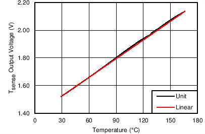
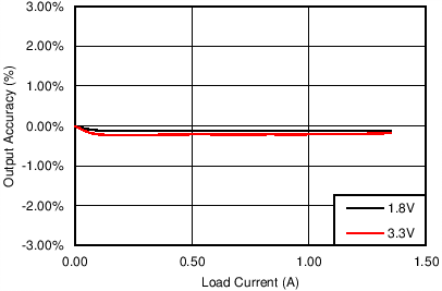
6.6 Typical Characteristics