SLRS063C September 2013 – February 2016 DRV8816
PRODUCTION DATA.
- 1 Features
- 2 Applications
- 3 Description
- 4 Revision History
- 5 Pin Configuration and Functions
- 6 Specifications
- 7 Detailed Description
- 8 Application and Implementation
- 9 Power Supply Recommendations
- 10Layout
- 11Device and Documentation Support
- 12Mechanical, Packaging, and Orderable Information
パッケージ・オプション
メカニカル・データ(パッケージ|ピン)
- PWP|16
サーマルパッド・メカニカル・データ
- PWP|16
発注情報
7 Detailed Description
7.1 Overview
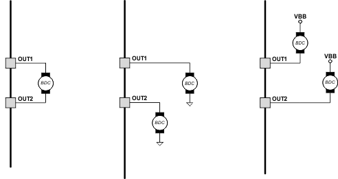
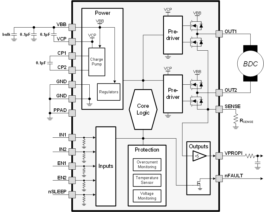
The DRV8816 uses 4 CMOS inputs to control 2 high-voltage high-current outputs, while integrating protection features, fault reporting, a sleep mode, and current sensing. EN1 and IN1 control OUT1, and EN2 and IN2 control OUT2, according to Table 2. The device is designed to drive two independent loads or one brushed DC motor, as shown in Figure 4 and Table 3.
When an RSENSE resistor is used, the DRV8816 will automatically disable itself if VSENSE exceeds 500mV—this provides a user-programmable overcurrent threshold. The VPROPI output equals the sense voltage amplified by a factor of 5, and it can be used by a microcontroller to know the motor current, in order to Pulse-Width Modulate the DRV8816 inputs and regulate motor current.
7.3 Feature Description
7.3.1 Bridge Control
The DRV8816 is controlled using separate enable and input pins for each ½-H-bridge.
Table 2 shows the logic for the DRV8816.
Table 2. DRV8816 Logic
| ENx | INx | OUTx |
|---|---|---|
| 0 | X | Z |
| 1 | 0 | L |
| 1 | 1 | H |
If a single DC motor is connected to the DRV8816, it is connected between the OUT1 and OUT2 pins as shown in Figure 4. Two DC motors may also be connected to the DRV8816. In this mode, it is not possible to reverse the direction of the motors; the motors will turn only in one direction. The connections are shown in Figure 4.
 Figure 4. Bridge Control
Table 3 shows how motor operation for a single-brushed DC motor is controlled.
Table 3. Motor Operation for a Single-Brushed DC Motor
| EN1 | EN2 | IN1 | IN2 | OUT1 | OUT2 | Operation |
|---|---|---|---|---|---|---|
| 0 | X | X | X | Z | X(1) | Off (coast) |
| X | 0 | X | X | X(1) | Z | Off (coast) |
| 1 | 1 | 0 | 0 | L | L | Brake |
| 1 | 1 | 0 | 1 | L | H | Reverse |
| 1 | 1 | 1 | 0 | H | L | Forward |
| 1 | 1 | 1 | 1 | H | H | Brake |
Table 4 shows how motor operation for dual-brushed DC motors is controlled.
Table 4. Motor Operation for a Dual-Brushed DC Motor
| Motor connected to GND | ENx | INx | OUTx | Operation |
| 0 | X | Z | Off (coast) | |
| 1 | 0 | L | Brake | |
| 1 | 1 | H | Forward | |
| Motor connected to VBB | ENx | INx | OUTx | Operation |
| 0 | X | Z | Off (coast) | |
| 1 | 0 | L | Forward | |
| 1 | 1 | H | Brake | |
7.3.2 Charge Pump
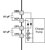
The charge pump is used to generate a supply above VBB to drive the source-side DMOS gates. A 0.1-μF ceramic monolithic capacitor should be connected between CP1 and CP2 for pumping purposes. A 0.1-μF ceramic monolithic capacitor should be connected between VCP and VBB to act as a reservoir to run the high-side DMOS devices. The VCP voltage level is internally monitored, and in the case of a fault condition, the outputs of the device are disabled.
 Figure 5. Charge Pump
7.3.3 VPROPI
The VPROPI output is equal to approximately 5× the voltage present on the SENSE pin. VPROPI is meaningful only if there is a resistor connected to the SENSE pin; If SENSE is connected to ground, VPROPI measures 0 V. Also note that during slow decay (brake), VPROPI measures 0 V. VPROPI can output a maximum of 2.5 V, because at 500 mV on SENSE, the H-bridge is disabled.
7.3.4 Protection Circuits
The DRV8816 is fully protected against VBB undervoltage, charge pump undervoltage, overcurrent, and overtemperature events.
7.3.4.1 VBB UVLO
If at any time the voltage on the VBB pin falls below the UVLO threshold voltage, all FETs in the H-bridge will be disabled and the charge pump will be disabled. Operation will resume when VBB rises above the UVLO threshold. Note that nFAULT does not indicate a UVLO because the CPUV fault is always asserted below VBB = 12 V.
7.3.4.2 VCP UVLO (CPUV)
During a CPUV event, the VCP voltage is measured to be below VCP + 10 V. If at any time the voltage on the VCP pin falls below the UVLO threshold voltage, the nFAULT pin is driven low. The nFAULT pin is released after operation has resumed. Note that this fault does not disable the output FETs and allows the device to continue operating. When VBB is below 12 V, this fault condition is always asserted and nFAULT is pulled low.
7.3.4.3 OCP
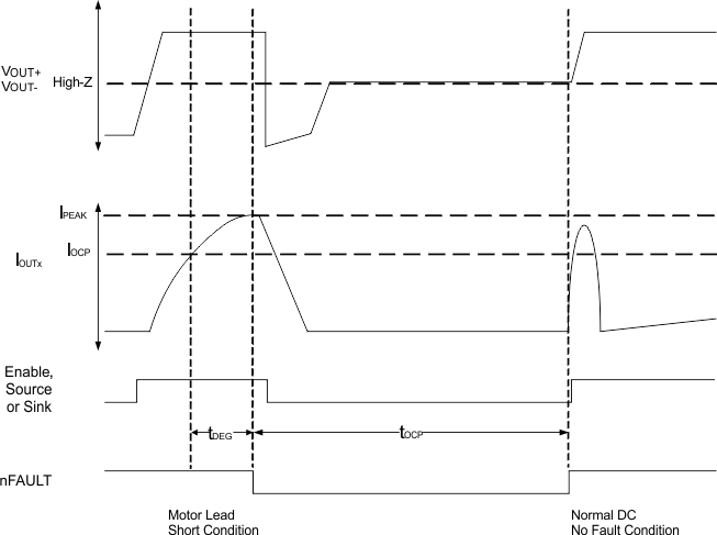
The current flowing through the high-side and low-side drivers is monitored to ensure that the motor lead is not shorted to supply or ground. If a short is detected, all FETs in the H-bridge are disabled, nFAULT is driven low, and a tOCP fault timer is started. After this period, tOCP, the device is then allowed to follow the input commands and another turn-on is attempted (nFAULT becomes high again during this attempt). If there is still a fault condition, the cycle repeats. If after tOCP expires it is determined the short condition is not present, normal operation resumes and nFAULT is released.
7.3.4.4 OTW
If the die temperature increases past the thermal warning threshold, the nFAULT pin is driven low. After the die temperature has fallen below the hysteresis level, the nFAULT pin is released. If the die temperature continues to increase, the device enters overtemperature shutdown as described in OTS .
7.3.4.5 OTS
If the die temperature exceeds safe limits, all FETs in the H-bridge are disabled and the charge pump is shut down. After the die temperature has fallen to a safe level, operation automatically resumes.
7.4 Device Functional Modes
7.4.1 SENSE
A low-value resistor can be placed between the SENSE pin and ground for current-sensing purposes. The PCB should be designed with wide metal paths on each side of the resistor, to minimize IR drop that would decrease sense accuracy. Likewise, the distance from the sense resistor to the DRV8816 and bulk capacitor should be minimized.
To set a manual overcurrent trip threshold, place a resistor between the SENSE pin and GND. When the SENSE pin rises above 500 mV, the H-bridge output is disabled (High-Z). The device will automatically retry with a period of tOCP. The overcurrent trip threshold can be calculated using ITRIP = 500 mV/Ω. The overcurrent trip level selected cannot be greater than IOCP.
If a sense resistor is not used, tie the SENSE pin directly to GND; in that case, the IOCP detection of current through the internal FETs still functions.

