SLVSAB2G May 2010 – December 2015 DRV8830
PRODUCTION DATA.
- 1 Features
- 2 Applications
- 3 Description
- 4 Revision History
- 5 Pin Configuration and Functions
- 6 Specifications
- 7 Detailed Description
- 8 Application and Implementation
- 9 Power Supply Recommendations
- 10Layout
- 11Device and Documentation Support
- 12Mechanical, Packaging, and Orderable Information
6 Specifications
6.1 Absolute Maximum Ratings
over operating free-air temperature range (unless otherwise noted)(1)(2)| MIN | MAX | UNIT | |||
|---|---|---|---|---|---|
| VCC | Power supply voltage | –0.3 | 7 | V | |
| Input pin voltage | –0.5 | 7 | V | ||
| Peak motor drive output current(3) | Internally limited | A | |||
| Continuous motor drive output current(3) | –1 | 1 | A | ||
| Continuous total power dissipation | See Thermal Information | ||||
| TJ | Operating virtual junction temperature | –40 | 150 | °C | |
| Tstg | Storage temperature | –60 | 150 | ||
(1) Stresses beyond those listed under Absolute Maximum Ratings may cause permanent damage to the device. These are stress ratings only, which do not imply functional operation of the device at these or any other conditions beyond those indicated under Recommended Operating Conditions. Exposure to absolute-maximum-rated conditions for extended periods may affect device reliability.
(2) All voltage values are with respect to network ground terminal.
(3) Power dissipation and thermal limits must be observed.
6.2 ESD Ratings
| VALUE | UNIT | |||
|---|---|---|---|---|
| V(ESD) | Electrostatic discharge | Human body model (HBM), per ANSI/ESDA/JEDEC JS-001(1) | ±2000 | V |
| Charged-device model (CDM), per JEDEC specification JESD22-C101(2) | ±1000 | |||
(1) JEDEC document JEP155 states that 500-V HBM allows safe manufacturing with a standard ESD control process.
(2) JEDEC document JEP157 states that 250-V CDM allows safe manufacturing with a standard ESD control process.
6.3 Recommended Operating Conditions
over operating free-air temperature range (unless otherwise noted)| MIN | MAX | UNIT | ||
|---|---|---|---|---|
| VCC | Motor power supply voltage | 2.75 | 6.8 | V |
| IOUT | Continuous or peak H-bridge output current(1) | 0 | 1 | A |
(1) Power dissipation and thermal limits must be observed.
6.4 Thermal Information
| THERMAL METRIC(1) | DRV8830 | UNIT | ||
|---|---|---|---|---|
| DGQ (HVSSOP) | DRC (VSON) | |||
| 10 PINS | 10 PINS | |||
| RθJA | Junction-to-ambient thermal resistance | 69.3 | 50.2 | °C/W |
| RθJC(top) | Junction-to-case (top) thermal resistance | 63.5 | 78.4 | °C/W |
| RθJB | Junction-to-board thermal resistance | 51.6 | 18.8 | °C/W |
| ψJT | Junction-to-top characterization parameter | 1.5 | 1.1 | °C/W |
| ψJB | Junction-to-board characterization parameter | 23.2 | 17.9 | °C/W |
| RθJB | Junction-to-case (bottom) thermal resistance | 9.5 | 5.1 | °C/W |
(1) For more information about traditional and new thermal metrics, see the Semiconductor and IC Package Thermal Metrics application report, SPRA953.
6.5 Electrical Characteristics
VCC = 2.75 V to 6.8 V, TA = –40°C to 85°C (unless otherwise noted)| PARAMETER | TEST CONDITIONS | MIN | TYP | MAX | UNIT | |
|---|---|---|---|---|---|---|
| POWER SUPPLIES | ||||||
| IVCC | VCC operating supply current | VCC = 5 V | 1.4 | 2 | mA | |
| IVCCQ | VCC sleep mode supply current | VCC = 5 V, TA = 25°C | 0.3 | 1 | μA | |
| VUVLO | VCC undervoltage lockout voltage | VCC rising | 2.575 | 2.75 | V | |
| VCC falling | 2.47 | |||||
| LOGIC-LEVEL INPUTS | ||||||
| VIL | Input low voltage | 0.25 × VCC | 0.38 × VCC | V | ||
| VIH | Input high voltage | 0.46 × VCC | 0.5 × VCC | V | ||
| VHYS | Input hysteresis | 0.08 × VCC | V | |||
| IIL | Input low current | VIN = 0 | –10 | 10 | μA | |
| IIH | Input high current | VIN = 3.3 V | 50 | μA | ||
| LOGIC-LEVEL OUTPUTS (FAULTn) | ||||||
| VOL | Output low voltage | IOL = 4 mA, VCC = 5 V | 0.5 | V | ||
| H-BRIDGE FETS | ||||||
| RDS(ON) | HS FET on resistance | VCC = 5 V, I O = 0.8 A, TJ = 85°C | 290 | 400 | mΩ | |
| VCC = 5 V, I O = 0.8 A, TJ = 25°C | 250 | |||||
| RDS(ON) | LS FET on resistance | VCC = 5 V, I O = 0.8 A, TJ = 85°C | 230 | 320 | mΩ | |
| VCC = 5 V, I O = 0.8 A, TJ = 25°C | 200 | |||||
| IOFF | Off-state leakage current | –20 | 20 | μA | ||
| MOTOR DRIVER | ||||||
| tR | Rise time | VCC = 3 V, load = 4 Ω | 50 | 300 | ns | |
| tF | Fall time | VCC = 3 V, load = 4 Ω | 50 | 300 | ns | |
| fSW | Internal PWM frequency | 44.5 | kHz | |||
| PROTECTION CIRCUITS | ||||||
| IOCP | Overcurrent protection trip level | 1.3 | 3 | A | ||
| tOCP | OCP deglitch time | 2 | μs | |||
| TTSD | Thermal shutdown temperature | Die temperature(1) | 150 | 160 | 180 | °C |
| VOLTAGE CONTROL | ||||||
| VREF | Reference output voltage | 1.235 | 1.285 | 1.335 | V | |
| ΔVLINE | Line regulation | VCC = 3.3 V to 6 V, VOUT = 3 V,(1)
IOUT = 500 mA |
±1% | |||
| ΔVLOAD | Load regulation | VCC = 5 V, VOUT = 3 V, IOUT = 200 mA to 800 mA(1) |
±1% | |||
| CURRENT LIMIT | ||||||
| VILIM | Current limit sense voltage | 160 | 200 | 240 | mV | |
| tILIM | Current limit fault deglitch time | 275 | ms | |||
| RISEN | Current limit sense resistance (external resistor value) | 0 | 1 | Ω | ||
(1) Not production tested.
6.6 I2C Timing Requirements(1)
VCC = 2.75 V to 6.8 V, TA = -40°C to 85°C (unless otherwise noted)| STANDARD MODE | FAST MODE | UNIT | ||||||
|---|---|---|---|---|---|---|---|---|
| MIN | NOM | MAX | MIN | NOM | MAX | |||
| fscl | I2C clock frequency | 0 | 100 | 0 | 400 | kHz | ||
| tsch | I2C clock high time | 4 | 0.6 | µs | ||||
| tscl | I2C clock low time | 4.7 | 1.3 | µs | ||||
| tsp | I2C spike time | 0 | 50 | 0 | 50 | ns | ||
| tsds | I2C serial data setup time | 250 | 100 | ns | ||||
| tsdh | I2C serial data hold time | 0 | 0 | ns | ||||
| ticr | I2C input rise time | 1000 | 20+0.1Cb(2) | 300 | ns | |||
| ticf | I2C input fall time | 300 | 20+0.1Cb(2) | 300 | ns | |||
| tocf | I2C output fall time | 300 | 20+0.1Cb(2) | 300 | ns | |||
| tbuf | I2C bus free time | 4.7 | 1.3 | µs | ||||
| tsts | I2C Start setup time | 4.7 | 0.6 | µs | ||||
| tsth | I2C Start hold time | 4 | 0.6 | µs | ||||
| tsps | I2C Stop setup time | 4 | 0.6 | µs | ||||
| tvd (data) | Valid data time (SCL low to SDA valid) | 1 | 1 | µs | ||||
| tvd (ack) | Valid data time of ACK (ACK signal from SCL low to SDA low) | 1 | 1 | µs | ||||
(1) Not production tested.
(2) Cb = total capacitance of one bus line in pF
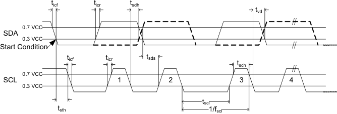 Figure 1. I2C Timing Requirements
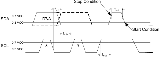 Figure 2. I2C Timing Requirements
6.7 Typical Characteristics
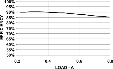 Figure 3. Efficiency vs Load Current
(VIN = 5 V, VOUT = 3 V)
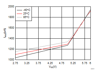 Figure 5. IVCC vs VVCC
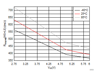 Figure 7. RDS(on) HS + LS vs VCC
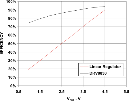 Figure 4. Efficiency vs Output Voltage
(VIN = 5 V, IOUT = 500 mA)
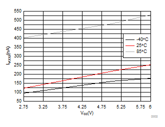 Figure 6. IVCCQ vs VVCC