SLVSAB8G May 2010 – March 2016 DRV8842
PRODUCTION DATA.
- 1 Features
- 2 Applications
- 3 Description
- 4 Revision History
- 5 Pin Configuration and Functions
- 6 Specifications
- 7 Detailed Description
- 8 Application and Implementation
- 9 Power Supply Recommendations
- 10Layout
- 11Device and Documentation Support
- 12Mechanical, Packaging, and Orderable Information
パッケージ・オプション
メカニカル・データ(パッケージ|ピン)
- PWP|28
サーマルパッド・メカニカル・データ
- PWP|28
発注情報
8 Application and Implementation
NOTE
Information in the following applications sections is not part of the TI component specification, and TI does not warrant its accuracy or completeness. TI’s customers are responsible for determining suitability of components for their purposes. Customers should validate and test their design implementation to confirm system functionality.
8.1 Application Information
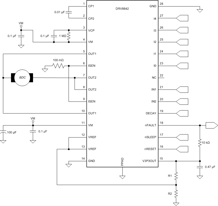
The DRV8842 device is used in brushed motor or stepper motor control. The onboard current regulation allows for limiting the motor current through simple pin configurations.
8.2 Typical Application
 Figure 7. Typical Application Schematic
8.2.1 Design Requirements
Table 3 shows the design parameters for this application.
Table 3. Design Parameters
| DESIGN PARAMETER | REFERENCE | EXAMPLE VALUE |
|---|---|---|
| Supply Voltage | VM | 24 V |
| Motor Winding Resistance | RM | 3.9 Ω |
| Motor Winding Inductance | LM | 2.9 mH |
| Target Chopping Current | ITRIP | 1.5 A |
| Sense Resistor | RSENSE | 100 mΩ |
| VREF Voltage | VREF | 0.75 V |
8.2.2 Detailed Design Procedure
8.2.2.1 Current Regulation
The maximum current (ITRIP) is set by the Ix pins, the VREF analog voltage, and the sense resistor value (RSENSE). When starting a brushed DC motor, a large inrush current may occur because there is no back-EMF and high detent torque. Current regulation will act to limit this inrush current and prevent high current on start-up.
Example: If the desired chopping currents is 1.5 A:
- Set RSENSE = 100 mΩ
- VREF would have to be 0.75 V
- Create a resistor divider network from V3P3OUT (3.3 V) to set VREF = 0.75 V
- Set R2 = 10 kΩ and set R1 = kΩ
8.2.2.2 Sense Resistor
For optimal performance, it is important for the sense resistor to be:
- Surface-mount
- Low inductance
- Rated for high enough power
- Placed closely to the motor driver
The power dissipated by the sense resistor equals Irms2 × R. For example, if the RMS motor current is 1.5 A and a 200-mΩ sense resistor is used, the resistor will dissipate 1.5 A2 × 0.2 Ω = 0.3 W. The power quickly increases with greater current levels.
Resistors typically have a rated power within some ambient temperature range, along with a derated power curve for high ambient temperatures. When a PCB is shared with other components generating heat, margin should be added. It is always best to measure the actual sense resistor temperature in a final system, along with the power MOSFETs, as those are often the hottest components.
Because power resistors are larger and more expensive than standard resistors, it is common practice to use multiple standard resistors in parallel, between the sense node and ground. This distributes the current and heat dissipation.
8.2.3 Application Curves
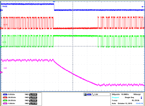
 Figure 8. DRV8842 Current Regulation
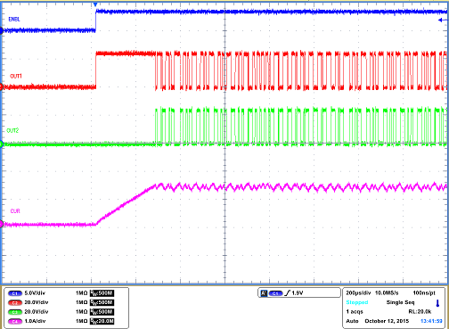
 Figure 9. DRV8842 Direction Change