JAJS617C July 1999 – July 2016 DS90LV048A
PRODUCTION DATA.
- 1 特長
- 2 アプリケーション
- 3 概要
- 4 改訂履歴
- 5 Pin Configuration and Functions
- 6 Specifications
- 7 Parameter Measurement Information
- 8 Detailed Description
- 9 Application and Implementation
- 10Power Supply Recommendations
- 11Layout
- 12デバイスおよびドキュメントのサポート
- 13メカニカル、パッケージ、および注文情報
パッケージ・オプション
メカニカル・データ(パッケージ|ピン)
サーマルパッド・メカニカル・データ
発注情報
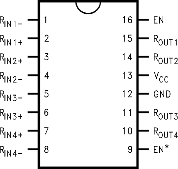
5 Pin Configuration and Functions
D or PW Package
16-Pin SOIC or TSSOP
Top View

Pin Functions
| PIN | I/O | DESCRIPTION | |
|---|---|---|---|
| NAME | NO. | ||
| EN | 16 | I | Receiver enable pin: When EN is low, the receiver is disabled. When EN is high and EN* is low or open, the receiver is enabled. If both EN and EN* are open circuit, then the receiver is disabled. |
| EN* | 9 | I | Receiver enable pin: When EN* is high, the receiver is disabled. When EN* is low or open and EN is high, the receiver is enabled. If both EN and EN* are open circuit, then the receiver is disabled. |
| GND | 12 | — | Ground pin |
| RIN+ | 2, 3, 6, 7 | I | Noninverting receiver input pin |
| RIN− | 1, 4, 5, 8 | I | Inverting receiver input pin |
| ROUT | 10, 11, 14, 15 | O | Receiver output pin |
| VCC | 13 | — | Power supply pin, +3.3V ± 0.3V |