SNLS336J October 2010 – November 2014 DS90UH925Q-Q1
PRODUCTION DATA.
- 1 Features
- 2 Applications
- 3 Description
- 4 Revision History
- 5 Pin Configuration and Functions
-
6 Specifications
- 6.1 Absolute Maximum Ratings
- 6.2 Handling Ratings
- 6.3 Recommended Operating Conditions
- 6.4 Thermal Information
- 6.5 DC Electrical Characteristics
- 6.6 AC Electrical Characteristics
- 6.7 DC and AC Serial Control Bus Characteristics
- 6.8 Recommended Timing for Serial Control Bus
- 6.9 Switching Characteristics
- 6.10 Typical Charateristics
-
7 Detailed Description
- 7.1 Overview
- 7.2 Functional Block Diagram
- 7.3
Feature Description
- 7.3.1 High Speed Forward Channel Data Transfer
- 7.3.2 Low Speed Back Channel Data Transfer
- 7.3.3 Backward Compatible Mode
- 7.3.4 Common Mode Filter Pin (CMF)
- 7.3.5 Video Control Signal Filter
- 7.3.6 Power Down (PDB)
- 7.3.7 Remote Auto Power Down Mode
- 7.3.8 LVCMOS VDDIO Option
- 7.3.9 Input PCLK Loss Detect
- 7.3.10 Serial Link Fault Detect
- 7.3.11 Pixel Clock Edge Select (RFB)
- 7.3.12 Low Frequency Optimization (LFMODE)
- 7.3.13 Interrupt Pin — Functional Description and Usage (INTB)
- 7.3.14 EMI Reduction Features
- 7.4 Device Functional Modes
- 7.5 Programming
- 7.6 Register Maps
- 8 Applications and Implementation
- 9 Power Supply Recommendations
- 10Layout
- 11Device and Documentation Support
- 12Mechanical, Packaging, and Orderable Information
パッケージ・オプション
メカニカル・データ(パッケージ|ピン)
- RHS|48
サーマルパッド・メカニカル・データ
- RHS|48
発注情報
5 Pin Configuration and Functions
48-Pin
Package RHS
(Top View)
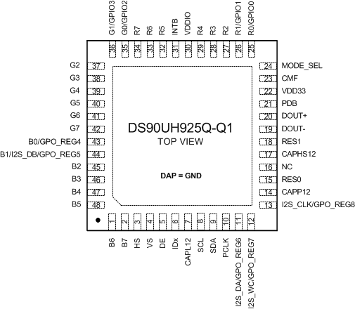
Pin Functions
| PIN | I/O, TYPE | DESCRIPTION | |
|---|---|---|---|
| NAME | NUMBER | ||
| LVCMOS PARALLEL INTERFACE | |||
| R[7:0] | 34, 33, 32, 29, 28, 27, 26, 25 | I, LVCMOS w/ pull down |
RED Parallel Interface Data Input Pins Leave open if unused. R0 can optionally be used as GPIO0 and R1 can optionally be used as GPIO1. |
| G[7:0] | 42, 41, 40, 39, 38, 37, 36, 35 | I, LVCMOS w/ pull down |
GREEN Parallel Interface Data Input Pins Leave open if unused. G0 can optionally be used as GPIO2 and G1 can optionally be used as GPIO3. |
| B[7:0] | 2, 1, 48, 47, 46, 45, 44, 43 | I, LVCOS w/ pull down |
BLUE Parallel Interface Data Input Pins Leave open if unused B0 can optionally be used as GPO_REG4 and B1 can optionally be used as GPO_REG5. |
| HS | 3 | I, LVCMOS w/ pull down |
Horizontal Sync Input Pin Video control signal pulse width must be 3 PCLKs or longer to be transmitted when the Control Signal Filter is enabled. There is no restriction on the minimum transition pulse when the Control Signal Filter is disabled. The signal is limited to 2 transitions per 130 PCLKs. See Table 6. |
| VS | 4 | I, LVCMOS w/ pull down |
Vertical Sync Input Pin Video control signal is limited to 1 transition per 130 PCLKs. Thus, the minimum pulse width is 130 PCLKs. |
| DE | 5 | I, LVCMOS w/ pull down |
Data Enable Input Pin Video control signal pulse width must be 3 PCLKs or longer to be transmitted when the Control Signal Filter is enabled. There is no restriction on the minimum transition pulse when the Control Signal Filter is disabled. The signal is limited to 2 transitions per 130 PCLKs. See Table 6. |
| PCLK | 10 | I, LVCMOS w/ pull down |
Pixel Clock Input Pin. Strobe edge set by RFB configuration register. See Table 6. |
| I2S_CLK, I2S_WC, I2S_DA | 13, 12, 11 | I, LVCMOS w/ pull down |
Digital Audio Interface Data Input Pins Leave open if unused. I2S_CLK can optionally be used as GPO_REG8, I2S_WC can optionally be used as GPO_REG7, and I2S_DA can optionally be used as GPO_REG6. |
| OPTIONAL PARALLEL INTERFACE | |||
| I2S_DB | 44 | I, LVCMOS w/ pull down |
Second Channel Digital Audio Interface Data Input pin at 18–bit color mode and set by MODE_SEL pin or configuration register Leave open if unused. I2S_DB can optionally be used as B1 or GPO_REG5. |
| GPIO[3:0] | 36, 35, 26, 25 | I/O, LVCMOS w/ pull down |
General Purpose IOs. Available only in 18-bit color mode, and set by MODE_SEL pin or configuration register. See Table 6. Leave open if unused Shared with G1, G0, R1 and R0. |
| GPO_REG[8:4] | 13, 12, 11, 44, 43 | O, LVCMOS w/ pull down |
General Purpose Outputs and set by configuration register. See Table 6. Share with I2S_CLK, I2S_WC, I2S_DA, I2S_DB or B1, B0. |
| CONTROL | |||
| PDB | 21 | I, LVCMOS w/ pull-down |
Power-down Mode Input Pin PDB = H, device is enabled (normal operation) Refer to ”Power Up Requirements and PDB Pin” in the Applications Information Section. PDB = L, device is powered down. When the device is in the powered down state, the Driver Outputs are both HIGH, the PLL is shutdown, and IDD is minimized. Control Registers are RESET. |
| MODE_SEL | 24 | I, Analog | Device Configuration Select. See Table 4. |
| I2C | |||
| IDx | 6 | I, Analog | I2C Serial Control Bus Device ID Address Select External pull-up to VDD33 is required under all conditions, DO NOT FLOAT. Connect to external pull-up and pull-down resistor to create a voltage divider. See Figure 19. |
| SCL | 8 | I/O, LVCMOS Open Drain |
I2C Clock Input / Output Interface Must have an external pull-up to VDD33, DO NOT FLOAT. Recommended pull-up: 4.7kΩ. |
| SDA | 9 | I/O, LVCMOS Open Drain |
I2C Data Input / Output Interface Must have an external pull-up to VDD33, DO NOT FLOAT. Recommended pull-up: 4.7kΩ. |
| STATUS | |||
| INTB | 31 | O, LVCMOS Open Drain |
HDCP Interrupt INTB = H, normal INTB = L, Interrupt request Recommended pull-up: 4.7kΩ to VDDIO |
| FPD-Link III SERIAL INTERFACE | |||
| DOUT+ | 20 | O, LVDS | True Output The output must be AC-coupled with a 0.1µF capacitor. |
| DOUT- | 19 | O, LVDS | Inverting Output The output must be AC-coupled with a 0.1µF capacitor. |
| CMF | 23 | Analog | Common Mode Filter. Connect 0.1µF to GND |
| POWER(1) and GROUND | |||
| VDD33 | 22 | Power | Power to on-chip regulator 3.0 V - 3.6 V. Requires 4.7 uF to GND |
| VDDIO | 30 | Power | LVCMOS I/O Power 1.8 V ±5% OR 3.0 V - 3.6 V. Requires 4.7 uF to GND |
| GND | DAP | Ground | DAP is the large metal contact at the bottom side, located at the center of the WQFN package. Connect to the ground plane (GND) with at least 9 vias. |
| REGULATOR CAPACITOR | |||
| CAPHS12, CAPP12 | 17, 14 | CAP | Decoupling capacitor connection for on-chip regulator. Requires a 4.7uF to GND at each CAP pin. |
| CAPL12 | 7 | CAP | Decoupling capacitor connection for on-chip regulator. Requires two 4.7uF to GND at this CAP pin. |
| OTHERS | |||
| NC | 16 | NC | Do not connect. |
| RES[1:0] | 18, 15 | GND | Reserved. Tie to Ground. |
(1) The VDD (VDD33 and VDDIO) supply ramp should be faster than 1.5 ms with a monotonic rise.