JAJSGJ0D October 2014 – February 2022 DS90UH948-Q1
PRODUCTION DATA
- 1 特長
- 2 アプリケーション
- 3 概要
- 4 Revision History
- 5 Pin Configuration and Functions
-
6 Specifications
- 6.1 Absolute Maximum Ratings
- 6.2 ESD Ratings
- 6.3 Recommended Operating Conditions
- 6.4 Thermal Information
- 6.5 DC Electrical Characteristics
- 6.6 AC Electrical Characteristics
- 6.7 Timing Requirements for the Serial Control Bus
- 6.8 Switching Characteristics
- 6.9 Timing Diagrams and Test Circuits
- 6.10 Typical Characteristics
-
7 Detailed Description
- 7.1 Overview
- 7.2 Functional Block Diagram
- 7.3
Feature Description
- 7.3.1 High-Speed Forward Channel Data Transfer
- 7.3.2 Low-Speed Back Channel Data Transfer
- 7.3.3 FPD-Link III Port Register Access
- 7.3.4 Oscillator Output
- 7.3.5 Clock and Output Status
- 7.3.6 LVCMOS VDDIO Option
- 7.3.7 Power Down (PDB)
- 7.3.8 Interrupt Pin — Functional Description and Usage (INTB_IN)
- 7.3.9 General-Purpose I/O (GPIO)
- 7.3.10 SPI Communication
- 7.3.11 Backward Compatibility
- 7.3.12 Adaptive Equalizer
- 7.3.13 I2S Audio Interface
- 7.3.14 HDCP Repeater
- 7.3.15 Built-In Self Test (BIST)
- 7.3.16 Internal Pattern Generation
- 7.4
Device Functional Modes
- 7.4.1
Configuration Select MODE_SEL[1:0]
- 7.4.1.1 1-Lane FPD-Link III Input, Single Link OpenLDI Output
- 7.4.1.2 1-Lane FPD-Link III Input, Dual Link OpenLDI Output
- 7.4.1.3 2-Lane FPD-Link III Input, Dual Link OpenLDI Output
- 7.4.1.4 2-Lane FPD-Link III Input, Single Link OpenLDI Output
- 7.4.1.5 1-Lane FPD-Link III Input, Single Link OpenLDI Output (Replicate)
- 7.4.2 MODE_SEL[1:0]
- 7.4.3 OpenLDI Output Frame and Color Bit Mapping Select
- 7.4.1
Configuration Select MODE_SEL[1:0]
- 7.5 Image Enhancement Features
- 7.6
Programming
- 7.6.1 Serial Control Bus
- 7.6.2 Multi-Controller Arbitration Support
- 7.6.3 I2C Restrictions on Multi-Controller Operation
- 7.6.4 Multi-Controller Access to Device Registers for Newer FPD-Link III Devices
- 7.6.5 Multi-Controller Access to Device Registers for Older FPD-Link III Devices
- 7.6.6 Restrictions on Control Channel Direction for Multi-Controller Operation
- 7.7 Register Maps
- 8 Application and Implementation
- 9 Power Supply Recommendations
- 10Layout
- 11Device and Documentation Support
- 12Mechanical, Packaging, and Orderable Information
パッケージ・オプション
メカニカル・データ(パッケージ|ピン)
- NKD|64
サーマルパッド・メカニカル・データ
- NKD|64
発注情報
7.3.14.2.1 Repeater Configuration
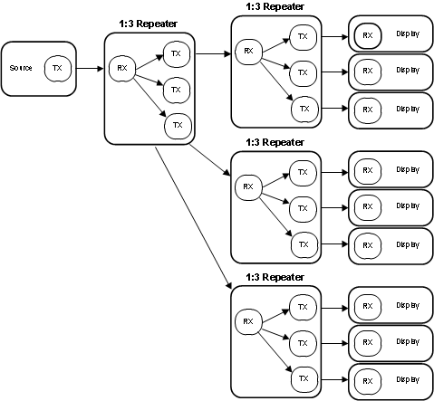
In the HDCP repeater application, this document refers to the DS90UH947-Q1 as the HDCP transmitter (TX), and refers to the DS90UH948-Q1 as the HDCP receiver (RX). #SNLS44049946 shows the maximum configuration supported for HDCP repeater implementations. Two levels of HDCP repeaters are supported with a maximum of three HDCP Transmitters per HDCP receiver.
 Figure 7-9 HDCP Maximum Repeater Application
In a repeater application, the I2C interface at each TX and RX is configured to transparently pass I2C communications upstream or downstream to any I2C device within the system. This includes a mechanism for assigning alternate IDs (Target Aliases) to downstream devices in the case of duplicate addresses.
To support HDCP repeater operation, the RX includes the ability to control the downstream authentication process, assemble the KSV list for downstream HDCP receivers, and pass the KSV list to the upstream HDCP transmitter. An I2C Controller within the RX communicates with the I2C Target within the TX. The TX handles authenticating with a downstream HDCP Receiver and makes status available through the I2C interface. The RX monitors the transmit port status for each TX and reads downstream KSV and KSV list values from the TX.
In addition to the I2C interface used to control the authentication process, the HDCP repeater implementation includes two other interfaces. The FPD-Link LVDS interface outputs the unencrypted video data. In addition to providing the video data, the LVDS interface communicates control information and packetized audio data. All audio and video data is decrypted at the output of the HDCP receiver and is re-encrypted by the HDCP transmitter. #SNLS44049954 provides more detailed block diagram of a 1:2 HDCP repeater configuration.
If the repeater node includes a local output to a display, white-balancing and Hi-FRC dithering functions must not be used as they will block encrypted I2S audio and HDCP authentication.